SNIS210G April   2019  – November 2023 TMP61-Q1

PRODUCTION DATA  

  1.   1
  2. Features
  3. Applications
  4. Description
  5. Device Comparison
  6. Pin Configuration and Functions
  7. Specifications
    1. 6.1 Absolute Maximum Ratings
    2. 6.2 ESD Ratings
    3. 6.3 Recommended Operating Conditions
    4. 6.4 Thermal Information
    5. 6.5 Electrical Characteristics
    6. 6.6 Typical Characteristics
  8. Detailed Description
    1. 7.1 Overview
    2. 7.2 Functional Block Diagram
    3. 7.3 Feature Description
      1. 7.3.1 TMP61-Q1 R-T table
      2. 7.3.2 Linear Resistance Curve
      3. 7.3.3 Positive Temperature Coefficient (PTC)
      4. 7.3.4 Built-In Fail Safe
    4. 7.4 Device Functional Modes
  9. Application and Implementation
    1. 8.1 Application Information
    2. 8.2 AEC-Q200 Qualifications
    3. 8.3 Typical Application
      1. 8.3.1 Thermistor Biasing Circuits
        1. 8.3.1.1 Design Requirements
        2. 8.3.1.2 Detailed Design Procedure
          1. 8.3.1.2.1 Thermal Protection With Comparator
          2. 8.3.1.2.2 Thermal Foldback
        3. 8.3.1.3 Application Curve
    4. 8.4 Power Supply Recommendations
    5. 8.5 Layout
      1. 8.5.1 Layout Guidelines
      2. 8.5.2 Layout Examples
  10. Device and Documentation Support
    1. 9.1 Documentation Support
      1. 9.1.1 Related Documentation
    2. 9.2 Receiving Notification of Documentation Updates
    3. 9.3 Support Resources
    4. 9.4 Trademarks
    5. 9.5 Glossary
    6. 9.6 Electrostatic Discharge Caution
  11. 10Revision History
  12. 11Mechanical, Packaging, and Orderable Information

Package Options

Mechanical Data (Package|Pins)
Thermal pad, mechanical data (Package|Pins)
Orderable Information

Typical Characteristics

at TA = 25°C, (unless otherwise noted)
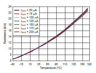
GUID-E2CD7A75-CF92-41E4-A8C4-AA4592DA3B87-low.gifFigure 6-1 Automotive Grade 0 Resistance vs Ambient Temperature Using Multiple Bias Currents
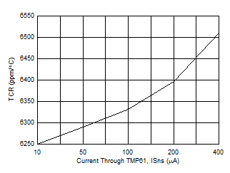
GUID-67E675CC-9DE0-438B-9BF7-200FC2A66683-low.gifFigure 6-3 TCR vs Sense Currents (ISNS)
GUID-20200917-CA0I-TV97-45N9-VWPKN25DVZR6-low.gif
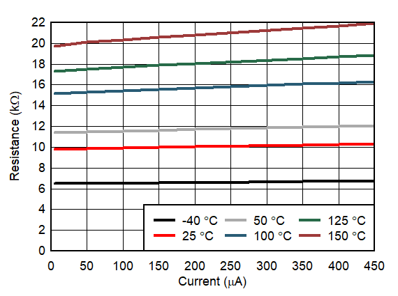
Figure 6-5 Supply Dependence Resistance vs Bias Current
GUID-72CBDE22-7ED3-4AC5-861A-0A9462535E21-low.gif
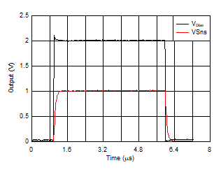
VSNS = 1 V
Figure 6-7 Step Response
GUID-1DC710CB-728A-4856-8CE5-0E678E6A7872-low.gif
Ambient condition: still air
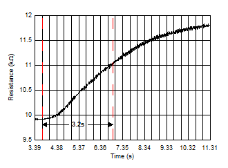
Figure 6-9 Thermal Response Time (DEC and DYA Package)
GUID-4FD45919-DB9A-43F0-9DC8-12C4AEE18405-low.gif
Ambient material: stirred liquid
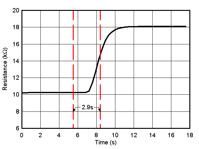
Figure 6-11 Thermal Response Time (LPG Package)
GUID-D92C9C33-BBF8-4A6E-98D9-889A4ADDC36B-low.gif
RBIAS = 10 kΩ with ±0.01% tolerance
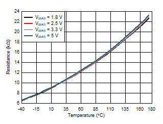
Figure 6-2 Automotive Grade 0 Resistance vs Ambient Temperature Using Multiple Bias Voltages
GUID-56FDFEBE-5939-43D3-AEE9-C9451A0D695B-low.gif
VSns = 1.8 V, 2.5 V, 3.3 V, and 5.0 V, RBias = 10 kΩ with ±0.01% Tolerance
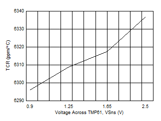
Figure 6-4 TCR vs Sense Voltages, VSns
GUID-20200917-CA0I-B6TD-D3TC-BSJW2WNHCMJW-low.gif
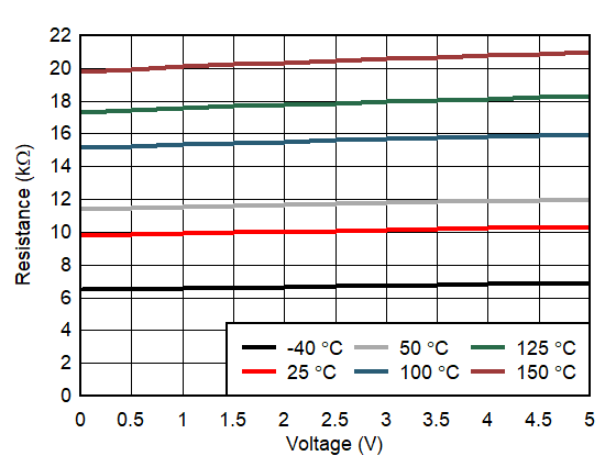
RBias = 10 kΩ ( ±0.01% tolerance)
Figure 6-6 Supply Dependence vs Bias Voltage
GUID-9F5A5702-CD14-4281-BBD3-0281EA00A71C-low.gif
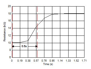
Ambient material: stirred liquid
Figure 6-8 Thermal Response Time (DEC package)
GUID-6E5DEB85-E67E-423C-B8C0-32009D34E0C7-low.gif
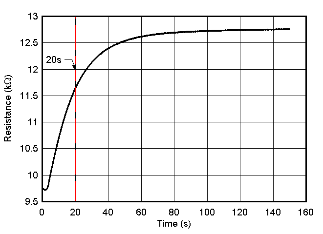
Ambient condition: still air
Figure 6-10 Thermal Response Time (LPG Package)