SNIS211D October 2019 – November 2020 TMP63
PRODUCTION DATA
- 1 Features
- 2 Applications
- 3 Description
- 4 Revision History
- 5 Device Comparison
- 6 Pin Configuration and Functions
- 7 Specifications
- 8 Detailed Description
- 9 Application and Implementation
- 10Power Supply Recommendations
- 11Layout
- 12Device and Documentation Support
- 13Mechanical, Packaging, and Orderable Information
Package Options
Mechanical Data (Package|Pins)
Thermal pad, mechanical data (Package|Pins)
Orderable Information
9.2.1.2 Detailed Design Procedure
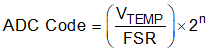
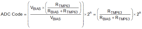
The resistive circuit divider method produces an output voltage (VTEMP) scaled according to the bias voltage (VBIAS). When VBIAS is also used as the reference voltage of the ADC, any fluctuations or tolerance error due to the voltage supply are canceled and do not affect the temperature accuracy (as shown in Figure 9-5). Equation 2 describes the output voltage (VTEMP) based on the variable resistance of the TMP63 (RTMP63) and bias resistor (RBIAS). The ADC code that corresponds to that output voltage, ADC full-scale range, and ADC resolution is given in Equation 3.
 Figure 9-5 Voltage Divider With an
ADC
Figure 9-5 Voltage Divider With an
ADC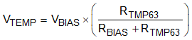
where
- FSR is the full-scale range of the ADC, which is the voltage at REF to GND (VREF)
- n is the resolution of the ADC
Equation 4 shows whenever VREF = VBIAS, VBIAS cancels out.
Use a polynomial equation or a LUT to extract the temperature reading based on the ADC code read in the microcontroller. Use the Thermistor Design Tool to translate the TMP63 resistance to temperature.
The cancellation of VBIAS is one benefit to using a voltage-divider (ratiometric approach), but the sensitivity of the output voltage of the divider circuit cannot increase much. Therefore, this application design does not use all of the ADC codes due to the small voltage output range compared to the FSR. This application is very common, however, and is simple to implement.
A current source-based circuit, such as the one shown in Figure 9-6, offers better control over the sensitivity of the output voltage and achieve higher accuracy. In this case, the output voltage is simply V = I × R. For example, if a current source of 40 µA is used with the device, the output voltage spans approximately 5.5 V and has a gain up to 40 mV/°C. Having control over the voltage range and sensitivity allows for full use of the ADC codes and full-scale range. Figure 9-11 shows the temperature voltage for various bias current conditions. Similar to the ratiometric approach, if the ADC has a built-in current source that shares the same bias as the reference voltage of the ADC, the tolerance of the supply current cancels out. In this case, a precision ADC is not required. This method yields the best accuracy, but can increase the system implementation cost.
 Figure 9-6 Biasing Circuit With Current
Source
Figure 9-6 Biasing Circuit With Current
SourceIn comparison to the non-linear NTC thermistor in a voltage divider, the TMP63 has an enhanced linear output characteristic. The two voltage divider circuits with and without a linearization parallel resistor, RP, are shown in Figure 9-7. Consider an example where VBIAS = 5 V, RBIAS = 100 kΩ, and a parallel resistor (RP) is used with the NTC thermistor (RNTC) to linearize the output voltage with an additional 100-kΩ resistor. The device produces a linear curve across the entire temperature range while the NTC curve is only linear across a small temperature region. When the parallel resistor (RP) is added to the NTC circuit, the added resistor makes the curve much more linear but greatly affects the output voltage range.
 Voltage Divider Circuits") Figure 9-7 TMP63 vs.
NTC With Linearization Resistor (RP) Voltage Divider Circuits
Figure 9-7 TMP63 vs.
NTC With Linearization Resistor (RP) Voltage Divider Circuits