SPRS565D April   2009  – June 2014 TMS320C6743

PRODUCTION DATA.  

  1. 1TMS320C6743 Fixed- and Floating-Point Digital Signal Processor
    1. 1.1 Features
    2. 1.2 Applications
    3. 1.3 Description
    4. 1.4 Functional Block Diagram
  2. 2Revision History
  3. 3Device Overview
    1. 3.1 Device Characteristics
    2. 3.2 Device Compatibility
    3. 3.3 DSP Subsystem
      1. 3.3.1 C674x DSP CPU Description
      2. 3.3.2 DSP Memory Mapping
        1. 3.3.2.1 External Memories
        2. 3.3.2.2 DSP Internal Memories
        3. 3.3.2.3 C674x CPU
    4. 3.4 Memory Map Summary
      1. 3.4.1 C6743 Top Level Memory Map
    5. 3.5 Pin Assignments
      1. 3.5.1 Pin Map (Bottom View)
    6. 3.6 Terminal Functions
      1. 3.6.1  Device Reset and JTAG
      2. 3.6.2  High-Frequency Oscillator and PLL
      3. 3.6.3  External Memory Interface A (ASYNC)
      4. 3.6.4  External Memory Interface B (SDRAM only)
      5. 3.6.5  Serial Peripheral Interface Modules (SPI0)
      6. 3.6.6  Enhanced Capture/Auxiliary PWM Modules (eCAP0, eCAP1, eCAP2)
      7. 3.6.7  Enhanced Pulse Width Modulators (eHRPWM0, eHRPWM1, eHRPWM2)
      8. 3.6.8  Enhanced Quadrature Encoder Pulse Module (eQEP)
      9. 3.6.9  Boot
      10. 3.6.10 Universal Asynchronous Receiver/Transmitters (UART0, UART2)
      11. 3.6.11 Inter-Integrated Circuit Modules (I2C0, I2C1)
      12. 3.6.12 Timers
      13. 3.6.13 Multichannel Audio Serial Ports (McASP0, McASP1)
      14. 3.6.14 Ethernet Media Access Controller (EMAC)
      15. 3.6.15 Multimedia Card/Secure Digital (MMC/SD)
      16. 3.6.16 General-Purpose IO Only Terminal Functions
      17. 3.6.17 Reserved and No Connect Terminal Functions
      18. 3.6.18 Supply and Ground Terminal Functions
  4. 4Device Configuration
    1. 4.1 Boot Modes
    2. 4.2 SYSCFG Module
    3. 4.3 Pullup/Pulldown Resistors
  5. 5Device Operating Conditions
    1. 5.1 Absolute Maximum Ratings Over Operating Junction Temperature Range (Unless Otherwise Noted)
    2. 5.2 Handling Ratings
    3. 5.3 Recommended Operating Conditions
    4. 5.4 Notes on Recommended Power-On Hours (POH)
    5. 5.5 Electrical Characteristics Over Recommended Ranges of Supply Voltage and Operating Junction Temperature (Unless Otherwise Noted)
  6. 6Peripheral Information and Electrical Specifications
    1. 6.1  Parameter Information
      1. 6.1.1 Parameter Information Device-Specific Information
        1. 6.1.1.1 Signal Transition Levels
    2. 6.2  Recommended Clock and Control Signal Transition Behavior
    3. 6.3  Power Supplies
      1. 6.3.1 Power-On Sequence
      2. 6.3.2 Power-Off Sequence
    4. 6.4  Reset
      1. 6.4.1 Power-On Reset (POR)
      2. 6.4.2 Warm Reset
      3. 6.4.3 Reset Electrical Data Timings
    5. 6.5  Crystal Oscillator or External Clock Input
    6. 6.6  Clock PLLs
      1. 6.6.1 PLL Device-Specific Information
      2. 6.6.2 Device Clock Generation
      3. 6.6.3 PLL Controller 0 Registers
    7. 6.7  DSP Interrupts
    8. 6.8  General-Purpose Input/Output (GPIO)
      1. 6.8.1 GPIO Register Description(s)
      2. 6.8.2 GPIO Peripheral Input/Output Electrical Data/Timing
        1. Table 6-10 Timing Requirements for GPIO Inputs (see )
        2. Table 6-11 Switching Characteristics Over Recommended Operating Conditions for GPIO Outputs (see )
      3. 6.8.3 GPIO Peripheral External Interrupts Electrical Data/Timing
        1. Table 6-12 Timing Requirements for External Interrupts (see )
    9. 6.9  EDMA
    10. 6.10 External Memory Interface A (EMIFA)
      1. 6.10.1 EMIFA Asynchronous Memory Support
      2. 6.10.2 EMIFA Connection Examples
      3. 6.10.3 External Memory Interface (EMIF) Registers
      4. 6.10.4 EMIFA Electrical Data/Timing
        1. Table 6-19 EMIFA Asynchronous Memory Timing Requirements
        2. Table 6-20 EMIFA Asynchronous Memory Switching Characteristics
    11. 6.11 External Memory Interface B (EMIFB)
      1. 6.11.1 EMIFB SDRAM Loading Limitations
      2. 6.11.2 Interfacing to SDRAM
      3. 6.11.3 EMIFB Electrical Data/Timing
        1. Table 6-24 EMIFB SDRAM Interface Timing Requirements
        2. Table 6-25 EMIFB SDRAM Interface Switching Characteristics
    12. 6.12 Memory Protection Units
    13. 6.13 MMC / SD / SDIO (MMCSD)
      1. 6.13.1 MMCSD Peripheral Register Description(s)
      2. 6.13.2 MMC/SD Electrical Data/Timing
        1. Table 6-29 Timing Requirements for MMC/SD Module (see and )
        2. Table 6-30 Switching Characteristics Over Recommended Operating Conditions for MMC/SD Module (see through )
    14. 6.14 Ethernet Media Access Controller (EMAC)
      1. 6.14.1 EMAC Peripheral Register Description(s)
      2. 6.14.2 EMAC Electrical Data/Timing
    15. 6.15 Management Data Input/Output (MDIO)
      1. 6.15.1 MDIO Peripheral Register Description(s)
      2. 6.15.2 Management Data Input/Output (MDIO) Electrical Data/Timing
        1. Table 6-38 Timing Requirements for MDIO Input (see and )
        2. Table 6-39 Switching Characteristics Over Recommended Operating Conditions for MDIO Output (see )
    16. 6.16 Multichannel Audio Serial Ports (McASP0, McASP1)
      1. 6.16.1 McASP Peripheral Registers Description(s)
      2. 6.16.2 McASP Electrical Data/Timing
        1. 6.16.2.1 Multichannel Audio Serial Port 0 (McASP0) Timing
          1. Table 6-44 McASP0 Timing Requirements
          2. Table 6-45 McASP0 Switching Characteristics
        2. 6.16.2.2 Multichannel Audio Serial Port 1 (McASP1) Timing
          1. Table 6-46 McASP1 Timing Requirements
          2. Table 6-47 McASP1 Switching Characteristics
    17. 6.17 Serial Peripheral Interface Ports (SPI0)
      1. 6.17.1 SPI Peripheral Registers Description(s)
      2. 6.17.2 SPI Electrical Data/Timing
        1. 6.17.2.1 Serial Peripheral Interface (SPI) Timing
          1. Table 6-49 General Timing Requirements for SPI0 Master Modes
          2. Table 6-50 General Timing Requirements for SPI0 Slave Modes
          3. Table 6-51 Additional SPI0 Master Timings, 4-Pin Enable Option
          4. Table 6-52 Additional SPI0 Master Timings, 4-Pin Chip Select Option
          5. Table 6-53 Additional SPI0 Master Timings, 5-Pin Option
          6. Table 6-54 Additional SPI0 Slave Timings, 4-Pin Enable Option
          7. Table 6-55 Additional SPI0 Slave Timings, 4-Pin Chip Select Option
          8. Table 6-56 Additional SPI0 Slave Timings, 5-Pin Option
    18. 6.18 Enhanced Capture (eCAP) Peripheral
      1. Table 6-58 Enhanced Capture (eCAP) Timing Requirement
      2. Table 6-59 eCAP Switching Characteristics
    19. 6.19 Enhanced Quadrature Encoder (eQEP) Peripheral
      1. Table 6-61 Enhanced Quadrature Encoder Pulse (eQEP) Timing Requirements
      2. Table 6-62 eQEP Switching Characteristics
    20. 6.20 Enhanced Pulse Width Modulator (eHRPWM) Modules
      1. 6.20.1 Enhanced Pulse Width Modulator (eHRPWM) Timing
        1. Table 6-64 eHRPWM Timing Requirements
        2. Table 6-65 eHRPWM Switching Characteristics
      2. 6.20.2 Trip-Zone Input Timing
    21. 6.21 Timers
      1. 6.21.1 Timer Electrical Data/Timing
        1. Table 6-69 Timing Requirements for Timer Input (see )
        2. Table 6-70 Switching Characteristics Over Recommended Operating Conditions for Timer Output
    22. 6.22 Inter-Integrated Circuit Serial Ports (I2C0, I2C1)
      1. 6.22.1 I2C Device-Specific Information
      2. 6.22.2 I2C Peripheral Registers Description(s)
      3. 6.22.3 I2C Electrical Data/Timing
        1. 6.22.3.1 Inter-Integrated Circuit (I2C) Timing
          1. Table 6-72 I2C Input Timing Requirements
          2. Table 6-73 I2C Switching Characteristics
    23. 6.23 Universal Asynchronous Receiver/Transmitter (UART)
      1. 6.23.1 UART Peripheral Registers Description(s)
      2. 6.23.2 UART Electrical Data/Timing
        1. Table 6-75 Timing Requirements for UARTx Receive (see )
        2. Table 6-76 Switching Characteristics Over Recommended Operating Conditions for UARTx Transmit (see )
    24. 6.24 Power and Sleep Controller (PSC)
      1. 6.24.1 PSC Peripheral Registers Description(s)
      2. 6.24.2 Power Domain and Module Topology
        1. 6.24.2.1 Power Domain States
        2. 6.24.2.2 Module States
    25. 6.25 Programmable Real-Time Unit Subsystem (PRUSS)
      1. 6.25.1 PRUSS Register Descriptions
    26. 6.26 Emulation Logic
      1. 6.26.1 JTAG Port Description
      2. 6.26.2 Scan Chain Configuration Parameters
      3. 6.26.3 JTAG 1149.1 Boundary Scan Considerations
    27. 6.27 IEEE 1149.1 JTAG
      1. 6.27.1 JTAG Peripheral Register Description(s) – JTAG ID Register
      2. 6.27.2 JTAG Test-Port Electrical Data/Timing
        1. Table 6-91 Timing Requirements for JTAG Test Port (see )
        2. Table 6-92 Switching Characteristics Over Recommended Operating Conditions for JTAG Test Port (see )
  7. 7Device and Documentation Support
    1. 7.1 Device Support
      1. 7.1.1 Development Support
      2. 7.1.2 Device and Development-Support Tool Nomenclature
    2. 7.2 Documentation Support
    3. 7.3 Support Resources
    4. 7.4 Trademarks
    5. 7.5 Electrostatic Discharge Caution
    6. 7.6 Glossary
  8. 8Mechanical Packaging and Orderable Information
    1. 8.1 Thermal Data for ZKB
    2. 8.2 Thermal Data for PTP
    3. 8.3 Supplementary Information About the 176-pin PTP PowerPAD™ Package
      1. 8.3.1 Standoff Height
      2. 8.3.2 PowerPAD™ PCB Footprint
    4. 8.4 Mechanical Drawings

Package Options

Refer to the PDF data sheet for device specific package drawings

Mechanical Data (Package|Pins)
  • ZKB|256
  • PTP|176
Thermal pad, mechanical data (Package|Pins)
Orderable Information

Device and Development-Support Tool Nomenclature

To designate the stages in the product development cycle, TI assigns prefixes to the part numbers of all DSP devices and support tools. Each DSP commercial family member has one of three prefixes: TMX, TMP, or TMS (e.g., TMS320C6743). Texas Instruments recommends two of three possible prefix designators for its support tools: TMDX and TMDS. These prefixes represent evolutionary stages of product development from engineering prototypes (TMX/TMDX) through fully qualified production devices/tools (TMS/TMDS).

Device development evolutionary flow:

    TMX Experimental device that is not necessarily representative of the final device's electrical specifications.
    TMP Final silicon die that conforms to the device's electrical specifications but has not completed quality and reliability verification.
    TMS Fully-qualified production device.

Support tool development evolutionary flow:

    TMDX Development-support product that has not yet completed Texas Instruments internal qualification testing.
    TMDS Fully qualified development-support product.

TMX and TMP devices and TMDX development-support tools are shipped against the following disclaimer:

"Developmental product is intended for internal evaluation purposes."

TMS devices and TMDS development-support tools have been characterized fully, and the quality and reliability of the device have been demonstrated fully. TI's standard warranty applies.

Predictions show that prototype devices (TMX or TMP) have a greater failure rate than the standard production devices. Texas Instruments recommends that these devices not be used in any production system because their expected end-use failure rate still is undefined. Only qualified production devices are to be used.

TI device nomenclature also includes a suffix with the device family name. This suffix indicates the package type (for example, ZWT), the temperature range (for example, "Blank" is the commercial temperature range), and the device speed range in megahertz (for example, "Blank" is the default).

Figure 7-1 provides a legend for reading the complete device name for any TMS320C674x member.
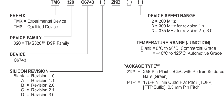
TMS320C6743 nomen_c6743_prs565.gif
BGA = Ball Grid Array.
Figure 7-1 Device Nomenclature