SPRS565D April 2009 – June 2014 TMS320C6743
PRODUCTION DATA.
- 1TMS320C6743 Fixed- and Floating-Point Digital Signal Processor
- 2Revision History
-
3Device Overview
- 3.1 Device Characteristics
- 3.2 Device Compatibility
- 3.3 DSP Subsystem
- 3.4 Memory Map Summary
- 3.5 Pin Assignments
- 3.6
Terminal Functions
- 3.6.1 Device Reset and JTAG
- 3.6.2 High-Frequency Oscillator and PLL
- 3.6.3 External Memory Interface A (ASYNC)
- 3.6.4 External Memory Interface B (SDRAM only)
- 3.6.5 Serial Peripheral Interface Modules (SPI0)
- 3.6.6 Enhanced Capture/Auxiliary PWM Modules (eCAP0, eCAP1, eCAP2)
- 3.6.7 Enhanced Pulse Width Modulators (eHRPWM0, eHRPWM1, eHRPWM2)
- 3.6.8 Enhanced Quadrature Encoder Pulse Module (eQEP)
- 3.6.9 Boot
- 3.6.10 Universal Asynchronous Receiver/Transmitters (UART0, UART2)
- 3.6.11 Inter-Integrated Circuit Modules (I2C0, I2C1)
- 3.6.12 Timers
- 3.6.13 Multichannel Audio Serial Ports (McASP0, McASP1)
- 3.6.14 Ethernet Media Access Controller (EMAC)
- 3.6.15 Multimedia Card/Secure Digital (MMC/SD)
- 3.6.16 General-Purpose IO Only Terminal Functions
- 3.6.17 Reserved and No Connect Terminal Functions
- 3.6.18 Supply and Ground Terminal Functions
- 4Device Configuration
-
5Device Operating Conditions
- 5.1 Absolute Maximum Ratings Over Operating Junction Temperature Range (Unless Otherwise Noted)
- 5.2 Handling Ratings
- 5.3 Recommended Operating Conditions
- 5.4 Notes on Recommended Power-On Hours (POH)
- 5.5 Electrical Characteristics Over Recommended Ranges of Supply Voltage and Operating Junction Temperature (Unless Otherwise Noted)
-
6Peripheral Information and Electrical Specifications
- 6.1 Parameter Information
- 6.2 Recommended Clock and Control Signal Transition Behavior
- 6.3 Power Supplies
- 6.4 Reset
- 6.5 Crystal Oscillator or External Clock Input
- 6.6 Clock PLLs
- 6.7 DSP Interrupts
- 6.8 General-Purpose Input/Output (GPIO)
- 6.9 EDMA
- 6.10 External Memory Interface A (EMIFA)
- 6.11 External Memory Interface B (EMIFB)
- 6.12 Memory Protection Units
- 6.13 MMC / SD / SDIO (MMCSD)
- 6.14 Ethernet Media Access Controller (EMAC)
- 6.15 Management Data Input/Output (MDIO)
- 6.16 Multichannel Audio Serial Ports (McASP0, McASP1)
- 6.17
Serial Peripheral Interface Ports (SPI0)
- 6.17.1 SPI Peripheral Registers Description(s)
- 6.17.2
SPI Electrical Data/Timing
- 6.17.2.1
Serial Peripheral Interface (SPI) Timing
- Table 6-49 General Timing Requirements for SPI0 Master Modes
- Table 6-50 General Timing Requirements for SPI0 Slave Modes
- Table 6-51 Additional SPI0 Master Timings, 4-Pin Enable Option
- Table 6-52 Additional SPI0 Master Timings, 4-Pin Chip Select Option
- Table 6-53 Additional SPI0 Master Timings, 5-Pin Option
- Table 6-54 Additional SPI0 Slave Timings, 4-Pin Enable Option
- Table 6-55 Additional SPI0 Slave Timings, 4-Pin Chip Select Option
- Table 6-56 Additional SPI0 Slave Timings, 5-Pin Option
- 6.17.2.1
Serial Peripheral Interface (SPI) Timing
- 6.18 Enhanced Capture (eCAP) Peripheral
- 6.19 Enhanced Quadrature Encoder (eQEP) Peripheral
- 6.20 Enhanced Pulse Width Modulator (eHRPWM) Modules
- 6.21 Timers
- 6.22 Inter-Integrated Circuit Serial Ports (I2C0, I2C1)
- 6.23 Universal Asynchronous Receiver/Transmitter (UART)
- 6.24 Power and Sleep Controller (PSC)
- 6.25 Programmable Real-Time Unit Subsystem (PRUSS)
- 6.26 Emulation Logic
- 6.27 IEEE 1149.1 JTAG
- 7Device and Documentation Support
- 8Mechanical Packaging and Orderable Information
Package Options
Refer to the PDF data sheet for device specific package drawings
Mechanical Data (Package|Pins)
- ZKB|256
- PTP|176
Thermal pad, mechanical data (Package|Pins)
- PTP|176
Orderable Information
6.19 Enhanced Quadrature Encoder (eQEP) Peripheral
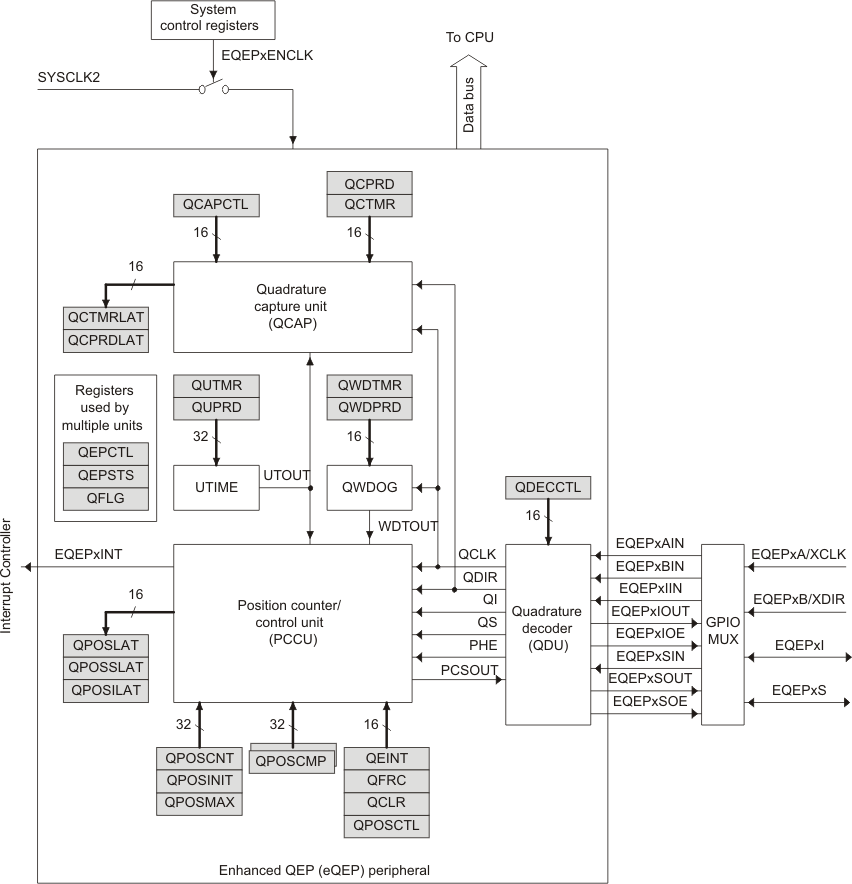
The device contains up to two enhanced quadrature encoder (eQEP) modules. See the TMS320C674x/OMAP-L1x Processor Peripherals Overview Reference Guide (SPRUFK9) for more details.
 Figure 6-38 eQEP Functional Block Diagram
 Table 6-60 is the list of the EQEP registers.
Table 6-61 shows the eQEP timing requirement and Table 6-62 shows the eQEP switching characteristics.
Table 6-60 EQEP Registers
| EQEP0
BYTE ADDRESS |
EQEP1
BYTE ADDRESS |
REGISTER NAME | REGISTER DESCRIPTION |
|---|---|---|---|
| 0x01F0 9000 | 0x01F0 A000 | QPOSCNT | eQEP Position Counter |
| 0x01F0 9004 | 0x01F0 A004 | QPOSINIT | eQEP Initialization Position Count |
| 0x01F0 9008 | 0x01F0 A008 | QPOSMAX | eQEP Maximum Position Count |
| 0x01F0 900C | 0x01F0 A00C | QPOSCMP | eQEP Position-compare |
| 0x01F0 9010 | 0x01F0 A010 | QPOSILAT | eQEP Index Position Latch |
| 0x01F0 9014 | 0x01F0 A014 | QPOSSLAT | eQEP Strobe Position Latch |
| 0x01F0 9018 | 0x01F0 A018 | QPOSLAT | eQEP Position Latch |
| 0x01F0 901C | 0x01F0 A01C | QUTMR | eQEP Unit Timer |
| 0x01F0 9020 | 0x01F0 A020 | QUPRD | eQEP Unit Period Register |
| 0x01F0 9024 | 0x01F0 A024 | QWDTMR | eQEP Watchdog Timer |
| 0x01F0 9026 | 0x01F0 A026 | QWDPRD | eQEP Watchdog Period Register |
| 0x01F0 9028 | 0x01F0 A028 | QDECCTL | eQEP Decoder Control Register |
| 0x01F0 902A | 0x01F0 A02A | QEPCTL | eQEP Control Register |
| 0x01F0 902C | 0x01F0 A02C | QCAPCTL | eQEP Capture Control Register |
| 0x01F0 902E | 0x01F0 A02E | QPOSCTL | eQEP Position-compare Control Register |
| 0x01F0 9030 | 0x01F0 A030 | QEINT | eQEP Interrupt Enable Register |
| 0x01F0 9032 | 0x01F0 A032 | QFLG | eQEP Interrupt Flag Register |
| 0x01F0 9034 | 0x01F0 A034 | QCLR | eQEP Interrupt Clear Register |
| 0x01F0 9036 | 0x01F0 A036 | QFRC | eQEP Interrupt Force Register |
| 0x01F0 9038 | 0x01F0 A038 | QEPSTS | eQEP Status Register |
| 0x01F0 903A | 0x01F0 A03A | QCTMR | eQEP Capture Timer |
| 0x01F0 903C | 0x01F0 A03C | QCPRD | eQEP Capture Period Register |
| 0x01F0 903E | 0x01F0 A03E | QCTMRLAT | eQEP Capture Timer Latch |
| 0x01F0 9040 | 0x01F0 A040 | QCPRDLAT | eQEP Capture Period Latch |
| 0x01F0 905C | 0x01F0 A05C | REVID | eQEP Revision ID |