SPRSP63B October   2022  – November 2023 TMS320F2800132 , TMS320F2800133 , TMS320F2800135 , TMS320F2800137

PRODUCTION DATA  

  1.   1
  2. Features
  3. Applications
  4. Description
    1. 3.1 Functional Block Diagram
  5. Device Comparison
    1. 4.1 Related Products
  6. Pin Configuration and Functions
    1. 5.1 Pin Diagrams
    2. 5.2 Pin Attributes
    3. 5.3 Signal Descriptions
      1. 5.3.1 Analog Signals
      2. 5.3.2 Digital Signals
      3. 5.3.3 Power and Ground
      4. 5.3.4 Test, JTAG, and Reset
    4. 5.4 Pin Multiplexing
      1. 5.4.1 GPIO Muxed Pins
        1. 5.4.1.1 GPIO Muxed Pins
      2. 5.4.2 Digital Inputs on ADC Pins (AIOs)
      3. 5.4.3 Digital Inputs and Outputs on ADC Pins (AGPIOs)
      4. 5.4.4 GPIO Input X-BAR
      5. 5.4.5 GPIO Output X-BAR and ePWM X-BAR
    5. 5.5 GPIO and ADC Allocation
    6. 5.6 Pins With Internal Pullup and Pulldown
    7. 5.7 Connections for Unused Pins
  7. Specifications
    1. 6.1  Absolute Maximum Ratings
    2. 6.2  ESD Ratings
    3. 6.3  Recommended Operating Conditions
    4. 6.4  Power Consumption Summary
      1. 6.4.1 System Current Consumption - VREG Enable - Internal Supply
      2. 6.4.2 System Current Consumption - VREG Disable - External Supply
      3. 6.4.3 Operating Mode Test Description
      4. 6.4.4 Current Consumption Graphs
      5. 6.4.5 Reducing Current Consumption
        1. 6.4.5.1 Typical Current Reduction per Disabled Peripheral
    5. 6.5  Electrical Characteristics
    6. 6.6  Thermal Resistance Characteristics for PM Package
    7. 6.7  Thermal Resistance Characteristics for PT Package
    8. 6.8  Thermal Resistance Characteristics for RGZ Package
    9. 6.9  Thermal Resistance Characteristics for RHB Package
    10. 6.10 Thermal Design Considerations
    11. 6.11 System
      1. 6.11.1  Power Management Module (PMM)
        1. 6.11.1.1 Introduction
        2. 6.11.1.2 Overview
          1. 6.11.1.2.1 Power Rail Monitors
            1. 6.11.1.2.1.1 I/O POR (Power-On Reset) Monitor
            2. 6.11.1.2.1.2 I/O BOR (Brown-Out Reset) Monitor
            3. 6.11.1.2.1.3 VDD POR (Power-On Reset) Monitor
          2. 6.11.1.2.2 External Supervisor Usage
          3. 6.11.1.2.3 Delay Blocks
          4. 6.11.1.2.4 Internal 1.2-V LDO Voltage Regulator (VREG)
          5. 6.11.1.2.5 VREGENZ
        3. 6.11.1.3 External Components
          1. 6.11.1.3.1 Decoupling Capacitors
            1. 6.11.1.3.1.1 VDDIO Decoupling
            2. 6.11.1.3.1.2 VDD Decoupling
        4. 6.11.1.4 Power Sequencing
          1. 6.11.1.4.1 Supply Pins Ganging
          2. 6.11.1.4.2 Signal Pins Power Sequence
          3. 6.11.1.4.3 Supply Pins Power Sequence
            1. 6.11.1.4.3.1 External VREG/VDD Mode Sequence
            2. 6.11.1.4.3.2 Internal VREG/VDD Mode Sequence
            3. 6.11.1.4.3.3 Supply Sequencing Summary and Effects of Violations
            4. 6.11.1.4.3.4 Supply Slew Rate
        5. 6.11.1.5 Recommended Operating Conditions Applicability to the PMM
        6. 6.11.1.6 Power Management Module Electrical Data and Timing
          1. 6.11.1.6.1 Power Management Module Operating Conditions
          2. 6.11.1.6.2 Power Management Module Characteristics
          3.        Supply Voltages
      2. 6.11.2  Reset Timing
        1. 6.11.2.1 Reset Sources
        2. 6.11.2.2 Reset Electrical Data and Timing
          1. 6.11.2.2.1 Reset - XRSn - Timing Requirements
          2. 6.11.2.2.2 Reset - XRSn - Switching Characteristics
          3. 6.11.2.2.3 Reset Timing Diagrams
      3. 6.11.3  Clock Specifications
        1. 6.11.3.1 Clock Sources
        2. 6.11.3.2 Clock Frequencies, Requirements, and Characteristics
          1. 6.11.3.2.1 Input Clock Frequency and Timing Requirements, PLL Lock Times
            1. 6.11.3.2.1.1 Input Clock Frequency
            2. 6.11.3.2.1.2 XTAL Oscillator Characteristics
            3. 6.11.3.2.1.3 X1 Input Level Characteristics When Using an External Clock Source - Not a Crystal
            4. 6.11.3.2.1.4 X1 Timing Requirements
            5. 6.11.3.2.1.5 AUXCLKIN Timing Requirements
            6. 6.11.3.2.1.6 APLL Characteristics
            7. 6.11.3.2.1.7 XCLKOUT Switching Characteristics - PLL Bypassed or Enabled
            8. 6.11.3.2.1.8 Internal Clock Frequencies
        3. 6.11.3.3 Input Clocks and PLLs
        4. 6.11.3.4 XTAL Oscillator
          1. 6.11.3.4.1 Introduction
          2. 6.11.3.4.2 Overview
            1. 6.11.3.4.2.1 Electrical Oscillator
              1. 6.11.3.4.2.1.1 Modes of Operation
                1. 6.11.3.4.2.1.1.1 Crystal Mode of Operation
                2. 6.11.3.4.2.1.1.2 Single-Ended Mode of Operation
              2. 6.11.3.4.2.1.2 XTAL Output on XCLKOUT
            2. 6.11.3.4.2.2 Quartz Crystal
            3. 6.11.3.4.2.3 GPIO Modes of Operation
          3. 6.11.3.4.3 Functional Operation
            1. 6.11.3.4.3.1 ESR – Effective Series Resistance
            2. 6.11.3.4.3.2 Rneg – Negative Resistance
            3. 6.11.3.4.3.3 Start-up Time
              1. 6.11.3.4.3.3.1 X1/X2 Precondition
            4. 6.11.3.4.3.4 DL – Drive Level
          4. 6.11.3.4.4 How to Choose a Crystal
          5. 6.11.3.4.5 Testing
          6. 6.11.3.4.6 Common Problems and Debug Tips
          7. 6.11.3.4.7 Crystal Oscillator Specifications
            1. 6.11.3.4.7.1 Crystal Oscillator Parameters
            2. 6.11.3.4.7.2 Crystal Equivalent Series Resistance (ESR) Requirements
            3. 6.11.3.4.7.3 Crystal Oscillator Electrical Characteristics
        5. 6.11.3.5 Internal Oscillators
          1. 6.11.3.5.1 INTOSC Characteristics
          2. 6.11.3.5.2 INTOSC2 with External Precision Resistor – ExtR
      4. 6.11.4  Flash Parameters
        1. 6.11.4.1 Flash Parameters 
      5. 6.11.5  RAM Specifications
      6. 6.11.6  ROM Specifications
      7. 6.11.7  Emulation/JTAG
        1. 6.11.7.1 JTAG Electrical Data and Timing
          1. 6.11.7.1.1 JTAG Timing Requirements
          2. 6.11.7.1.2 JTAG Switching Characteristics
          3. 6.11.7.1.3 JTAG Timing Diagram
        2. 6.11.7.2 cJTAG Electrical Data and Timing
          1. 6.11.7.2.1 cJTAG Timing Requirements
          2. 6.11.7.2.2 cJTAG Switching Characteristics
          3. 6.11.7.2.3 cJTAG Timing Diagram
      8. 6.11.8  GPIO Electrical Data and Timing
        1. 6.11.8.1 GPIO – Output Timing
          1. 6.11.8.1.1 General-Purpose Output Switching Characteristics
          2. 6.11.8.1.2 General-Purpose Output Timing Diagram
        2. 6.11.8.2 GPIO – Input Timing
          1. 6.11.8.2.1 General-Purpose Input Timing Requirements
          2. 6.11.8.2.2 Sampling Mode
        3. 6.11.8.3 Sampling Window Width for Input Signals
      9. 6.11.9  Interrupts
        1. 6.11.9.1 External Interrupt (XINT) Electrical Data and Timing
          1. 6.11.9.1.1 External Interrupt Timing Requirements
          2. 6.11.9.1.2 External Interrupt Switching Characteristics
          3. 6.11.9.1.3 External Interrupt Timing
      10. 6.11.10 Low-Power Modes
        1. 6.11.10.1 Clock-Gating Low-Power Modes
        2. 6.11.10.2 Low-Power Mode Wake-up Timing
          1. 6.11.10.2.1 IDLE Mode Timing Requirements
          2. 6.11.10.2.2 IDLE Mode Switching Characteristics
          3. 6.11.10.2.3 IDLE Entry and Exit Timing Diagram
          4. 6.11.10.2.4 STANDBY Mode Timing Requirements
          5. 6.11.10.2.5 STANDBY Mode Switching Characteristics
          6. 6.11.10.2.6 STANDBY Entry and Exit Timing Diagram
          7. 6.11.10.2.7 HALT Mode Timing Requirements
          8. 6.11.10.2.8 HALT Mode Switching Characteristics
          9. 6.11.10.2.9 HALT Entry and Exit Timing Diagram
    12. 6.12 Analog Peripherals
      1. 6.12.1 Analog Pins and Internal Connections
      2. 6.12.2 Analog Signal Descriptions
      3. 6.12.3 Analog-to-Digital Converter (ADC)
        1. 6.12.3.1 ADC Configurability
          1. 6.12.3.1.1 Signal Mode
        2. 6.12.3.2 ADC Electrical Data and Timing
          1. 6.12.3.2.1 ADC Operating Conditions
          2. 6.12.3.2.2 ADC Characteristics
          3. 6.12.3.2.3 ADC Performance Per Pin
          4. 6.12.3.2.4 ADC Input Model
          5. 6.12.3.2.5 ADC Timing Diagrams
      4. 6.12.4 Temperature Sensor
        1. 6.12.4.1 Temperature Sensor Electrical Data and Timing
          1. 6.12.4.1.1 Temperature Sensor Characteristics
      5. 6.12.5 Comparator Subsystem (CMPSS)
        1. 6.12.5.1 CMPSS Module Variants
        2. 6.12.5.2 CMPx_DACL
        3. 6.12.5.3 CMPSS Connectivity Diagram
        4. 6.12.5.4 Block Diagrams
        5. 6.12.5.5 CMPSS Electrical Data and Timing
          1. 6.12.5.5.1 CMPSS Comparator Electrical Characteristics
          2. 6.12.5.5.2 CMPSS_LITE Comparator Electrical Characteristics
          3.        CMPSS Comparator Input Referred Offset and Hysteresis
          4. 6.12.5.5.3 CMPSS DAC Static Electrical Characteristics
          5. 6.12.5.5.4 CMPSS_LITE DAC Static Electrical Characteristics
          6. 6.12.5.5.5 CMPSS Illustrative Graphs
          7. 6.12.5.5.6 CMPSS DAC Dynamic Error
          8. 6.12.5.5.7 Buffered Output from CMPx_DACL Operating Conditions
          9. 6.12.5.5.8 Buffered Output from CMPx_DACL Electrical Characteristics
    13. 6.13 Control Peripherals
      1. 6.13.1 Enhanced Pulse Width Modulator (ePWM)
        1. 6.13.1.1 Control Peripherals Synchronization
        2. 6.13.1.2 ePWM Electrical Data and Timing
          1. 6.13.1.2.1 ePWM Timing Requirements
          2. 6.13.1.2.2 ePWM Switching Characteristics
          3. 6.13.1.2.3 Trip-Zone Input Timing
            1. 6.13.1.2.3.1 Trip-Zone Input Timing Requirements
            2. 6.13.1.2.3.2 PWM Hi-Z Characteristics Timing Diagram
      2. 6.13.2 High-Resolution Pulse Width Modulator (HRPWM)
        1. 6.13.2.1 HRPWM Electrical Data and Timing
          1. 6.13.2.1.1 High-Resolution PWM Characteristics
      3. 6.13.3 External ADC Start-of-Conversion Electrical Data and Timing
        1. 6.13.3.1 External ADC Start-of-Conversion Switching Characteristics
        2. 6.13.3.2 ADCSOCAO or ADCSOCBO Timing Diagram
      4. 6.13.4 Enhanced Capture (eCAP)
        1. 6.13.4.1 eCAP Block Diagram
        2. 6.13.4.2 eCAP Synchronization
        3. 6.13.4.3 eCAP Electrical Data and Timing
          1. 6.13.4.3.1 eCAP Timing Requirements
          2. 6.13.4.3.2 eCAP Switching Characteristics
      5. 6.13.5 Enhanced Quadrature Encoder Pulse (eQEP)
        1. 6.13.5.1 eQEP Electrical Data and Timing
          1. 6.13.5.1.1 eQEP Timing Requirements
          2. 6.13.5.1.2 eQEP Switching Characteristics
    14. 6.14 Communications Peripherals
      1. 6.14.1 Controller Area Network (CAN)
      2. 6.14.2 Inter-Integrated Circuit (I2C)
        1. 6.14.2.1 I2C Electrical Data and Timing
          1. 6.14.2.1.1 I2C Timing Requirements
          2. 6.14.2.1.2 I2C Switching Characteristics
          3. 6.14.2.1.3 I2C Timing Diagram
      3. 6.14.3 Serial Communications Interface (SCI)
      4. 6.14.4 Serial Peripheral Interface (SPI)
        1. 6.14.4.1 SPI Master Mode Timings
          1. 6.14.4.1.1 SPI Master Mode Timing Requirements
          2. 6.14.4.1.2 SPI Master Mode Switching Characteristics - Clock Phase 0
          3. 6.14.4.1.3 SPI Master Mode Switching Characteristics - Clock Phase 1
          4. 6.14.4.1.4 SPI Master Mode Timing Diagrams
        2. 6.14.4.2 SPI Slave Mode Timings
          1. 6.14.4.2.1 SPI Slave Mode Timing Requirements
          2. 6.14.4.2.2 SPI Slave Mode Switching Characteristics
          3. 6.14.4.2.3 SPI Slave Mode Timing Diagrams
  8. Detailed Description
    1. 7.1  Overview
    2. 7.2  Functional Block Diagram
    3. 7.3  Memory
      1. 7.3.1 Memory Map
        1. 7.3.1.1 Dedicated RAM (Mx RAM)
        2. 7.3.1.2 Local Shared RAM (LSx RAM)
      2. 7.3.2 Flash Memory Map
      3. 7.3.3 Peripheral Registers Memory Map
    4. 7.4  Identification
    5. 7.5  C28x Processor
      1. 7.5.1 Floating-Point Unit (FPU)
      2. 7.5.2 Trigonometric Math Unit (TMU)
    6. 7.6  Device Boot Modes
      1. 7.6.1 Device Boot Configurations
        1. 7.6.1.1 Configuring Boot Mode Pins
        2. 7.6.1.2 Configuring Boot Mode Table Options
      2. 7.6.2 GPIO Assignments
    7. 7.7  Security
      1. 7.7.1 Securing the Boundary of the Chip
        1. 7.7.1.1 JTAGLOCK
        2. 7.7.1.2 Zero-pin Boot
      2. 7.7.2 Dual-Zone Security
      3. 7.7.3 Disclaimer
    8. 7.8  Watchdog
    9. 7.9  C28x Timers
    10. 7.10 Dual-Clock Comparator (DCC)
      1. 7.10.1 Features
      2. 7.10.2 Mapping of DCCx Clock Source Inputs
  9. Applications, Implementation, and Layout
    1. 8.1 Application and Implementation
    2. 8.2 Key Device Features
    3. 8.3 Application Information
      1. 8.3.1 Typical Applications
        1. 8.3.1.1 Air-conditioner Outdoor Unit
          1. 8.3.1.1.1 System Block Diagram
          2. 8.3.1.1.2 Air Conditioner Outdoor Unit Resources
        2. 8.3.1.2 Washer and Dryer
          1. 8.3.1.2.1 System Block Diagram
          2. 8.3.1.2.2 Washer and Dryer Resources
        3. 8.3.1.3 Robotic Lawn Mower
          1. 8.3.1.3.1 System Block Diagram
          2. 8.3.1.3.2 Robotic Lawn Mower Resources
        4. 8.3.1.4 Merchant Telecom Rectifiers
          1. 8.3.1.4.1 System Block Diagram
          2. 8.3.1.4.2 Merchant Telecom Rectifiers Resources
  10. Device and Documentation Support
    1. 9.1 Getting Started and Next Steps
    2. 9.2 Device Nomenclature
    3. 9.3 Markings
    4. 9.4 Tools and Software
    5. 9.5 Documentation Support
    6. 9.6 Support Resources
    7. 9.7 Trademarks
    8. 9.8 Electrostatic Discharge Caution
    9. 9.9 Glossary
  11. 10Revision History
  12. 11Mechanical, Packaging, and Orderable Information

Package Options

Refer to the PDF data sheet for device specific package drawings

Mechanical Data (Package|Pins)
  • PM|64
  • RGZ|48
  • RHB|32
  • PT|48
Thermal pad, mechanical data (Package|Pins)
Orderable Information
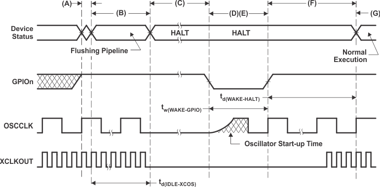
HALT Entry and Exit Timing Diagram
GUID-20210426-CA0I-MKHQ-2JH2-WHHLM72FRHDD-low.gif
IDLE instruction is executed to put the device into HALT mode.
The LPM block responds to the HALT signal, SYSCLK is held for a maximum 16 INTOSC1 clock cycles before being turned off. This delay enables the CPU pipeline and any other pending operations to flush properly.
Clocks to the peripherals are turned off and the PLL is shut down. If a quartz crystal or ceramic resonator is used as the clock source, the internal oscillator is shut down as well. The device is now in HALT mode and consumes very little power. It is possible to keep the internal oscillators (INTOSC1 and INTOSC2) and the watchdog alive in HALT MODE. This is done by writing 1 to CLKSRCCTL1.WDHALTI. After the IDLE instruction is executed, a delay of five OSCCLK cycles (minimum) is needed before the wake-up signal could be asserted.
When the GPIOn pin (used to bring the device out of HALT) is driven low, the oscillator is turned on and the oscillator wake-up sequence is initiated. The GPIO pin should be driven high only after the oscillator has stabilized. This enables the provision of a clean clock signal during the PLL lock sequence. Because the falling edge of the GPIO pin asynchronously begins the wake-up procedure, care should be taken to maintain a low noise environment before entering and during HALT mode.
The wake-up signal fed to a GPIO pin to wake up the device must meet the minimum pulse width requirement. Furthermore, this signal must be free of glitches. If a noisy signal is fed to a GPIO pin, the wake-up behavior of the device will not be deterministic and the device may not exit low-power mode for subsequent wake-up pulses.
When CLKIN to the core is enabled, the device will respond to the interrupt (if enabled), after some latency. The HALT mode is now exited.
Normal operation resumes.
The user must relock the PLL upon HALT wakeup to ensure a stable PLL lock.
Figure 6-36 HALT Entry and Exit Timing Diagram