SPRS945G January   2017  – January 2023 TMS320F280040-Q1 , TMS320F280040C-Q1 , TMS320F280041 , TMS320F280041-Q1 , TMS320F280041C , TMS320F280041C-Q1 , TMS320F280045 , TMS320F280048-Q1 , TMS320F280048C-Q1 , TMS320F280049 , TMS320F280049-Q1 , TMS320F280049C , TMS320F280049C-Q1

PRODUCTION DATA  

  1. Features
  2. Applications
  3. Description
    1. 3.1 Functional Block Diagram
  4. Revision History
  5. Device Comparison
    1. 5.1 Related Products
  6. Pin Configuration and Functions
    1. 6.1 Pin Diagrams
    2. 6.2 Pin Attributes
    3. 6.3 Signal Descriptions
      1. 6.3.1 Analog Signals
      2. 6.3.2 Digital Signals
      3. 6.3.3 Power and Ground
      4. 6.3.4 Test, JTAG, and Reset
    4. 6.4 Pin Multiplexing
      1. 6.4.1 GPIO Muxed Pins
      2. 6.4.2 Digital Inputs on ADC Pins (AIOs)
      3. 6.4.3 GPIO Input X-BAR
      4. 6.4.4 GPIO Output X-BAR and ePWM X-BAR
    5. 6.5 Pins With Internal Pullup and Pulldown
    6. 6.6 Connections for Unused Pins
  7. Specifications
    1. 7.1  Absolute Maximum Ratings
    2. 7.2  ESD Ratings – Commercial
    3. 7.3  ESD Ratings – Automotive
    4. 7.4  Recommended Operating Conditions
    5. 7.5  Power Consumption Summary
      1. 7.5.1 System Current Consumption (External Supply)
      2. 7.5.2 System Current Consumption (Internal VREG)
      3. 7.5.3 System Current Consumption (DCDC)
      4. 7.5.4 Operating Mode Test Description
      5. 7.5.5 Current Consumption Graphs
      6. 7.5.6 Reducing Current Consumption
        1. 7.5.6.1 Typical IDD Current Reduction per Disabled Peripheral (at 100-MHz SYSCLK)
    6. 7.6  Electrical Characteristics
    7. 7.7  Thermal Resistance Characteristics
      1. 7.7.1 PZ Package
      2. 7.7.2 PM Package
      3. 7.7.3 RSH Package
    8. 7.8  Thermal Design Considerations
    9. 7.9  System
      1. 7.9.1 Power Management Module (PMM)
        1. 7.9.1.1 Introduction
        2. 7.9.1.2 Overview
          1. 7.9.1.2.1 Power Rail Monitors
            1. 7.9.1.2.1.1 I/O POR (Power-On Reset) Monitor
            2. 7.9.1.2.1.2 I/O BOR (Brown-Out Reset) Monitor
            3. 7.9.1.2.1.3 VDD POR (Power-On Reset) Monitor
          2. 7.9.1.2.2 External Supervisor Usage
          3. 7.9.1.2.3 Delay Blocks
          4. 7.9.1.2.4 Internal 1.2-V LDO Voltage Regulator (VREG)
          5. 7.9.1.2.5 VREGENZ
          6. 7.9.1.2.6 Internal 1.2-V Switching Regulator (DC-DC)
            1. 7.9.1.2.6.1 PCB Layout and Component Guidelines
        3. 7.9.1.3 External Components
          1. 7.9.1.3.1 Decoupling Capacitors
            1. 7.9.1.3.1.1 VDDIO Decoupling
            2. 7.9.1.3.1.2 VDD Decoupling
        4. 7.9.1.4 Power Sequencing
          1. 7.9.1.4.1 Supply Pins Ganging
          2. 7.9.1.4.2 Signal Pins Power Sequence
          3. 7.9.1.4.3 Supply Pins Power Sequence
            1. 7.9.1.4.3.1 External VREG/VDD Mode Sequence
            2. 7.9.1.4.3.2 Internal VREG/VDD Mode Sequence
            3. 7.9.1.4.3.3 Supply Sequencing Summary and Effects of Violations
            4. 7.9.1.4.3.4 Supply Slew Rate
        5. 7.9.1.5 Power Management Module Electrical Data and Timing
          1. 7.9.1.5.1 Power Management Module Operating Conditions
          2. 7.9.1.5.2 Power Management Module Characteristics
          3.        Supply Voltages
      2. 7.9.2 Reset Timing
        1. 7.9.2.1 Reset Sources
        2. 7.9.2.2 Reset Electrical Data and Timing
          1. 7.9.2.2.1 Reset (XRSn) Timing Requirements
          2. 7.9.2.2.2 Reset (XRSn) Switching Characteristics
          3. 7.9.2.2.3 Reset Timing Diagram
      3. 7.9.3 Clock Specifications
        1. 7.9.3.1 Clock Sources
        2. 7.9.3.2 Clock Frequencies, Requirements, and Characteristics
          1. 7.9.3.2.1 Input Clock Frequency and Timing Requirements, PLL Lock Times
            1. 7.9.3.2.1.1 Input Clock Frequency
            2. 7.9.3.2.1.2 XTAL Oscillator Characteristics
            3. 7.9.3.2.1.3 X1 Timing Requirements
            4. 7.9.3.2.1.4 PLL Lock Times
          2. 7.9.3.2.2 Internal Clock Frequencies
            1. 7.9.3.2.2.1 Internal Clock Frequencies
          3. 7.9.3.2.3 Output Clock Frequency and Switching Characteristics
            1. 7.9.3.2.3.1 XCLKOUT Switching Characteristics
        3. 7.9.3.3 Input Clocks and PLLs
        4. 7.9.3.4 Crystal (XTAL) Oscillator
          1. 7.9.3.4.1 Introduction
          2. 7.9.3.4.2 Overview
            1. 7.9.3.4.2.1 Electrical Oscillator
              1. 7.9.3.4.2.1.1 Modes of Operation
                1. 7.9.3.4.2.1.1.1 Crystal Mode of Operation
                2. 7.9.3.4.2.1.1.2 Single-Ended Mode of Operation
              2. 7.9.3.4.2.1.2 XTAL Output on XCLKOUT
            2. 7.9.3.4.2.2 Quartz Crystal
            3. 7.9.3.4.2.3 GPIO Modes of Operation
          3. 7.9.3.4.3 Functional Operation
            1. 7.9.3.4.3.1 ESR – Effective Series Resistance
            2. 7.9.3.4.3.2 Rneg – Negative Resistance
            3. 7.9.3.4.3.3 Start-up Time
            4. 7.9.3.4.3.4 DL – Drive Level
          4. 7.9.3.4.4 How to Choose a Crystal
          5. 7.9.3.4.5 Testing
          6. 7.9.3.4.6 Common Problems and Debug Tips
          7. 7.9.3.4.7 Crystal Oscillator Specifications
            1. 7.9.3.4.7.1 Crystal Oscillator Parameters
            2. 7.9.3.4.7.2 Crystal Equivalent Series Resistance (ESR) Requirements
            3. 7.9.3.4.7.3 Crystal Oscillator Electrical Characteristics
        5. 7.9.3.5 Internal Oscillators
          1. 7.9.3.5.1 INTOSC Characteristics
      4. 7.9.4 Flash Parameters
      5. 7.9.5 Emulation/JTAG
        1. 7.9.5.1 JTAG Electrical Data and Timing
          1. 7.9.5.1.1 JTAG Timing Requirements
          2. 7.9.5.1.2 JTAG Switching Characteristics
          3. 7.9.5.1.3 JTAG Timing Diagram
        2. 7.9.5.2 cJTAG Electrical Data and Timing
          1. 7.9.5.2.1 cJTAG Timing Requirements
          2. 7.9.5.2.2 cJTAG Switching Characteristics
          3. 7.9.5.2.3 cJTAG Timing Diagram
      6. 7.9.6 GPIO Electrical Data and Timing
        1. 7.9.6.1 GPIO – Output Timing
          1. 7.9.6.1.1 General-Purpose Output Switching Characteristics
        2. 7.9.6.2 GPIO – Input Timing
          1. 7.9.6.2.1 General-Purpose Input Timing Requirements
        3. 7.9.6.3 Sampling Window Width for Input Signals
      7. 7.9.7 Interrupts
        1. 7.9.7.1 External Interrupt (XINT) Electrical Data and Timing
          1. 7.9.7.1.1 External Interrupt Timing Requirements
          2. 7.9.7.1.2 External Interrupt Switching Characteristics
          3. 7.9.7.1.3 Interrupt Timing Diagram
      8. 7.9.8 Low-Power Modes
        1. 7.9.8.1 Clock-Gating Low-Power Modes
        2. 7.9.8.2 Low-Power Mode Wake-up Timing
          1. 7.9.8.2.1 IDLE Mode Timing Requirements
          2. 7.9.8.2.2 IDLE Mode Switching Characteristics
          3. 7.9.8.2.3 IDLE Mode Timing Diagram
          4. 7.9.8.2.4 HALT Mode Timing Requirements
          5. 7.9.8.2.5 HALT Mode Switching Characteristics
          6. 7.9.8.2.6 HALT Mode Timing Diagram
    10. 7.10 Analog Peripherals
      1. 7.10.1 Analog-to-Digital Converter (ADC)
        1. 7.10.1.1 Result Register Mapping
        2. 7.10.1.2 ADC Configurability
          1. 7.10.1.2.1 Signal Mode
        3. 7.10.1.3 ADC Electrical Data and Timing
          1. 7.10.1.3.1 ADC Operating Conditions
          2. 7.10.1.3.2 ADC Characteristics
          3. 7.10.1.3.3 ADC Input Model
          4. 7.10.1.3.4 ADC Timing Diagrams
      2. 7.10.2 Programmable Gain Amplifier (PGA)
        1. 7.10.2.1 PGA Electrical Data and Timing
          1. 7.10.2.1.1 PGA Operating Conditions
          2. 7.10.2.1.2 PGA Characteristics
          3. 7.10.2.1.3 PGA Typical Characteristics Graphs
      3. 7.10.3 Temperature Sensor
        1. 7.10.3.1 Temperature Sensor Electrical Data and Timing
          1. 7.10.3.1.1 Temperature Sensor Characteristics
      4. 7.10.4 Buffered Digital-to-Analog Converter (DAC)
        1. 7.10.4.1 Buffered DAC Electrical Data and Timing
          1. 7.10.4.1.1 Buffered DAC Operating Conditions
          2. 7.10.4.1.2 Buffered DAC Electrical Characteristics
          3. 7.10.4.1.3 Buffered DAC Illustrative Graphs
          4. 7.10.4.1.4 Buffered DAC Typical Characteristics Graphs
      5. 7.10.5 Comparator Subsystem (CMPSS)
        1. 7.10.5.1 CMPSS Electrical Data and Timing
          1. 7.10.5.1.1 Comparator Electrical Characteristics
          2. 7.10.5.1.2 CMPSS DAC Static Electrical Characteristics
          3. 7.10.5.1.3 CMPSS Illustrative Graphs
    11. 7.11 Control Peripherals
      1. 7.11.1 Enhanced Capture (eCAP)
        1. 7.11.1.1 eCAP Electrical Data and Timing
          1. 7.11.1.1.1 eCAP Timing Requirements
          2. 7.11.1.1.2 eCAP Switching Characteristics
      2. 7.11.2 High-Resolution Capture Submodule (HRCAP6–HRCAP7)
        1. 7.11.2.1 HRCAP Electrical Data and Timing
          1. 7.11.2.1.1 HRCAP Switching Characteristics
      3. 7.11.3 Enhanced Pulse Width Modulator (ePWM)
        1. 7.11.3.1 Control Peripherals Synchronization
        2. 7.11.3.2 ePWM Electrical Data and Timing
          1. 7.11.3.2.1 ePWM Timing Requirements
          2. 7.11.3.2.2 ePWM Switching Characteristics
          3. 7.11.3.2.3 Trip-Zone Input Timing
            1. 7.11.3.2.3.1 Trip-Zone Input Timing Requirements
        3. 7.11.3.3 External ADC Start-of-Conversion Electrical Data and Timing
          1. 7.11.3.3.1 External ADC Start-of-Conversion Switching Characteristics
      4. 7.11.4 High-Resolution Pulse Width Modulator (HRPWM)
        1. 7.11.4.1 HRPWM Electrical Data and Timing
          1. 7.11.4.1.1 High-Resolution PWM Characteristics
      5. 7.11.5 Enhanced Quadrature Encoder Pulse (eQEP)
        1. 7.11.5.1 eQEP Electrical Data and Timing
          1. 7.11.5.1.1 eQEP Timing Requirements
          2. 7.11.5.1.2 eQEP Switching Characteristics
      6. 7.11.6 Sigma-Delta Filter Module (SDFM)
        1. 7.11.6.1 SDFM Electrical Data and Timing
          1. 7.11.6.1.1 SDFM Timing Requirements When Using Asynchronous GPIO (ASYNC) Option
          2. 7.11.6.1.2 SDFM Timing Diagram
        2. 7.11.6.2 SDFM Electrical Data and Timing (Synchronized GPIO)
          1. 7.11.6.2.1 SDFM Timing Requirements When Using Synchronized GPIO (SYNC) Option
    12. 7.12 Communications Peripherals
      1. 7.12.1 Controller Area Network (CAN)
      2. 7.12.2 Inter-Integrated Circuit (I2C)
        1. 7.12.2.1 I2C Electrical Data and Timing
          1. 7.12.2.1.1 I2C Timing Requirements
          2. 7.12.2.1.2 I2C Switching Characteristics
          3. 7.12.2.1.3 I2C Timing Diagram
      3. 7.12.3 Power Management Bus (PMBus) Interface
        1. 7.12.3.1 PMBus Electrical Data and Timing
          1. 7.12.3.1.1 PMBus Electrical Characteristics
          2. 7.12.3.1.2 PMBus Fast Mode Switching Characteristics
          3. 7.12.3.1.3 PMBus Standard Mode Switching Characteristics
      4. 7.12.4 Serial Communications Interface (SCI)
      5. 7.12.5 Serial Peripheral Interface (SPI)
        1. 7.12.5.1 SPI Electrical Data and Timing
          1. 7.12.5.1.1 Non-High-Speed Master Mode Timings
            1. 7.12.5.1.1.1 SPI Master Mode Switching Characteristics (Clock Phase = 0)
            2. 7.12.5.1.1.2 SPI Master Mode Switching Characteristics (Clock Phase = 1)
            3. 7.12.5.1.1.3 SPI Master Mode Timing Requirements
          2. 7.12.5.1.2 Non-High-Speed Slave Mode Timings
            1. 7.12.5.1.2.1 SPI Slave Mode Switching Characteristics
            2. 7.12.5.1.2.2 SPI Slave Mode Timing Requirements
          3. 7.12.5.1.3 High-Speed Master Mode Timings
            1. 7.12.5.1.3.1 SPI High-Speed Master Mode Switching Characteristics (Clock Phase = 0)
            2. 7.12.5.1.3.2 SPI High-Speed Master Mode Switching Characteristics (Clock Phase = 1)
            3. 7.12.5.1.3.3 SPI High-Speed Master Mode Timing Requirements
          4. 7.12.5.1.4 High-Speed Slave Mode Timings
            1. 7.12.5.1.4.1 SPI High-Speed Slave Mode Switching Characteristics
            2. 7.12.5.1.4.2 SPI High-Speed Slave Mode Timing Requirements
      6. 7.12.6 Local Interconnect Network (LIN)
      7. 7.12.7 Fast Serial Interface (FSI)
        1. 7.12.7.1 FSI Transmitter
          1. 7.12.7.1.1 FSITX Electrical Data and Timing
            1. 7.12.7.1.1.1 FSITX Switching Characteristics
        2. 7.12.7.2 FSI Receiver
          1. 7.12.7.2.1 FSIRX Electrical Data and Timing
            1. 7.12.7.2.1.1 FSIRX Switching Characteristics
            2. 7.12.7.2.1.2 FSIRX Timing Requirements
        3. 7.12.7.3 FSI SPI Compatibility Mode
          1. 7.12.7.3.1 FSITX SPI Signaling Mode Electrical Data and Timing
            1. 7.12.7.3.1.1 FSITX SPI Signaling Mode Switching Characteristics
  8. Detailed Description
    1. 8.1  Overview
    2. 8.2  Functional Block Diagram
    3. 8.3  Memory
      1. 8.3.1 C28x Memory Map
      2. 8.3.2 Control Law Accelerator (CLA) ROM Memory Map
      3. 8.3.3 Flash Memory Map
      4. 8.3.4 Peripheral Registers Memory Map
      5. 8.3.5 Memory Types
        1. 8.3.5.1 Dedicated RAM (Mx RAM)
        2. 8.3.5.2 Local Shared RAM (LSx RAM)
        3. 8.3.5.3 Global Shared RAM (GSx RAM)
        4. 8.3.5.4 CLA Message RAM (CLA MSGRAM)
    4. 8.4  Identification
    5. 8.5  Bus Architecture – Peripheral Connectivity
    6. 8.6  C28x Processor
      1. 8.6.1 Embedded Real-Time Analysis and Diagnostic (ERAD)
      2. 8.6.2 Floating-Point Unit (FPU)
      3. 8.6.3 Trigonometric Math Unit (TMU)
      4. 8.6.4 Viterbi, Complex Math and CRC Unit (VCU-I)
    7. 8.7  Control Law Accelerator (CLA)
    8. 8.8  Direct Memory Access (DMA)
    9. 8.9  Boot ROM and Peripheral Booting
      1. 8.9.1 Configuring Alternate Boot Mode Select Pins
      2. 8.9.2 Configuring Alternate Boot Mode Options
      3. 8.9.3 GPIO Assignments
    10. 8.10 Dual Code Security Module
    11. 8.11 Watchdog
    12. 8.12 Configurable Logic Block (CLB)
    13. 8.13 Functional Safety
  9. Applications, Implementation, and Layout
    1. 9.1 Key Device Features
    2. 9.2 Application Information
      1. 9.2.1 Typical Application
        1. 9.2.1.1 Server Telecom Power Supply Unit (PSU)
          1. 9.2.1.1.1 System Block Diagram
          2. 9.2.1.1.2 Server and Telecom PSU Resources
        2. 9.2.1.2 Single-Phase Online UPS
          1. 9.2.1.2.1 System Block Diagram
          2. 9.2.1.2.2 Single phase online UPS Resources
        3. 9.2.1.3 Solar Micro Inverter
          1. 9.2.1.3.1 System Block Diagram
          2. 9.2.1.3.2 Solar Micro Inverter Resources
        4. 9.2.1.4 EV Charging Station Power Module
          1. 9.2.1.4.1 System Block Diagram
          2. 9.2.1.4.2 EV charging station power module Resources
        5. 9.2.1.5 Servo Drive Control Module
          1. 9.2.1.5.1 System Block Diagram
          2. 9.2.1.5.2 Servo Drive Control Module Resources
  10. 10Device and Documentation Support
    1. 10.1 Device and Development Support Tool Nomenclature
    2. 10.2 Markings
    3. 10.3 Tools and Software
    4. 10.4 Documentation Support
    5. 10.5 Support Resources
    6. 10.6 Trademarks
    7. 10.7 Electrostatic Discharge Caution
    8. 10.8 Glossary
  11. 11Mechanical, Packaging, and Orderable Information
    1. 11.1 Packaging Information

Package Options

Mechanical Data (Package|Pins)
Thermal pad, mechanical data (Package|Pins)
Orderable Information

Analog Peripherals

The analog subsystem module is described in this section.

The analog modules on this device include the ADC, PGA, temperature sensor, buffered DAC, and CMPSS.

The analog subsystem has the following features:

  • Flexible voltage references
    • The ADCs are referenced to VREFHIx and VREFLOx pins.
      • VREFHIx pin voltage can be driven in externally or can be generated by an internal bandgap voltage reference.
      • The internal voltage reference range can be selected to be 0 V to 3.3 V or 0 V to 2.5 V.
  • The buffered DACs are referenced to VREFHIx and VREFLOx.
    • Alternately, these DACs can be referenced to the VDAC pin and VSSA.
  • The comparator DACs are referenced to VDDA and VSSA.
    • Alternately, these DACs can be referenced to the VDAC pin and VSSA.
  • Flexible pin usage
    • Buffered DAC outputs, comparator subsystem inputs, PGA functions, and digital inputs are multiplexed with ADC inputs
    • Internal connection to VREFLO on all ADCs for offset self-calibration

Figure 7-37 shows the Analog Subsystem Block Diagram for the 100-pin PZ LQFP.

Figure 7-38 shows the Analog Subsystem Block Diagram for the 64-pin PM LQFP.

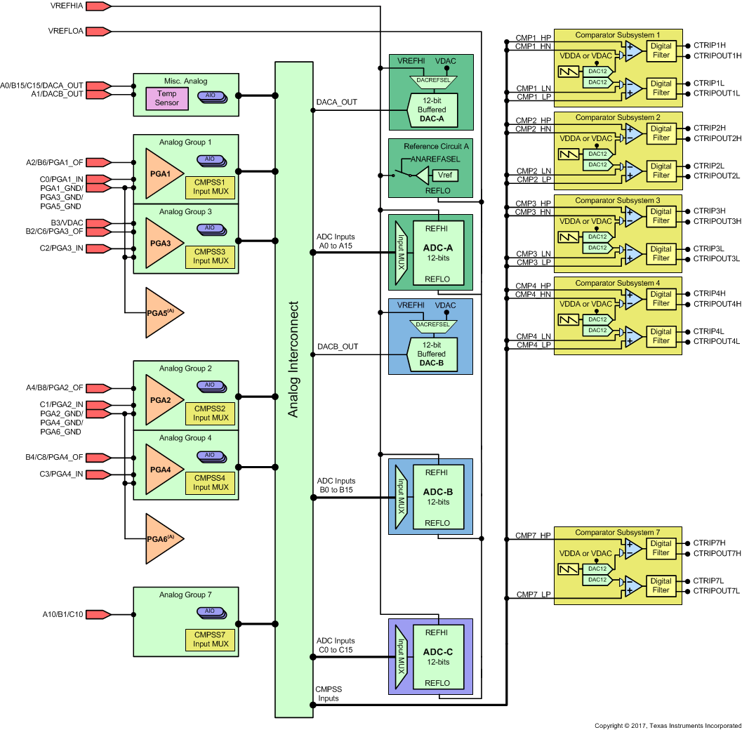
Figure 7-39 shows the Analog Subsystem Block Diagram for the 56-pin RSH VQFN.
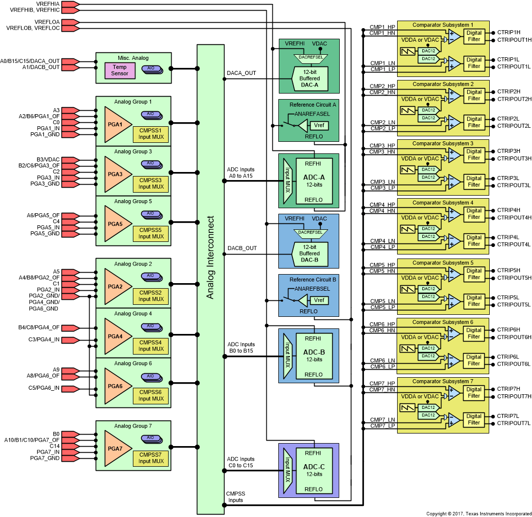
GUID-D33716C9-C91C-4FD9-ABD0-80803F83FBEE-low.gif Figure 7-37 Analog Subsystem Block Diagram (100-Pin PZ LQFP)
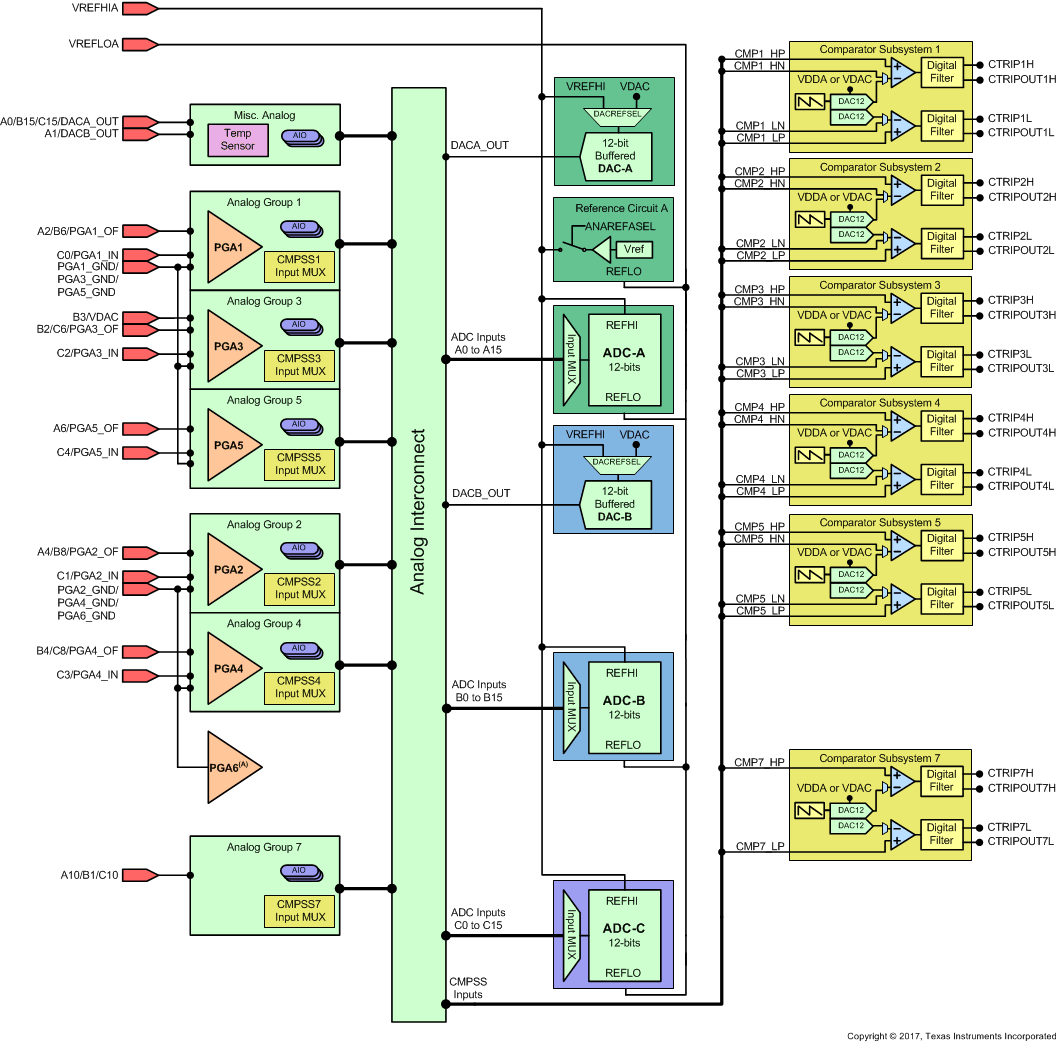
GUID-D3E1382E-139E-44D4-BCDB-5B7DDDB99459-low.gif
This PGA has no input/output connections on this package, but should be enabled and disabled at the same time as other PGAs with a shared PGA ground.
Figure 7-38 Analog Subsystem Block Diagram (64-Pin PM LQFP)
GUID-0323E7AE-2B87-48CC-87BB-0931BF6739FF-low.gif
This PGA has no input/output connections on this package, but should be enabled and disabled at the same time as other PGAs with a shared PGA ground.
Figure 7-39 Analog Subsystem Block Diagram (56-Pin RSH VQFN)

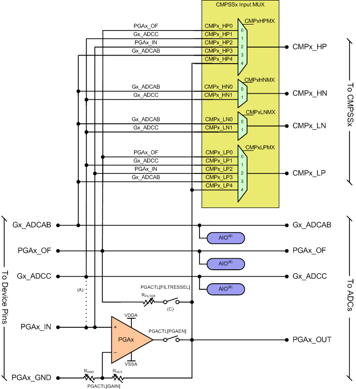
Figure 7-40 shows the analog group connections. See the Analog Pins and Internal Connections table for the specific connections for each group for each package. The Analog Signal Descriptions table provides descriptions of the analog signals.
GUID-06135FBD-EFF1-45DB-A2BC-1ABE38313BCE-low.gif
On lower pin-count packages, the input to Gx_ADCC will share a pin with the PGA input. If the PGA input is unused, then the ADCC input can allow the pin to be used as an ADC input, a negative comparator input, or a digital input.
AIOs support digital input mode only.
The PGA RFILTER path is not available on some device revisions. See the TMS320F28004x Real-Time MCUs Silicon Errata for more information.
Figure 7-40 Analog Group Connections
Table 7-13 Analog Pins and Internal Connections
PIN NAMEGROUP NAMEPACKAGEALWAYS CONNECTED (NO MUX)COMPARATOR SUBSYSTEM (MUX)AIO INPUT
100 PZ64 PM56 RSHADCAADCBADCCPGADACHIGH POSITIVEHIGH NEGATIVELOW POSITIVELOW NEGATIVE
VREFHIA-251614
VREFHIB-24
VREFHIC-
VREFLOA-271715A13
VREFLOB-26B13
VREFLOC-C13
Analog Group 1CMP1
A3G1_ADCAB10A3HPMXSEL = 3HNMXSEL = 0LPMXSEL = 3LNMXSEL = 0AIO233
A2/B6/PGA1_OFPGA1_OF998A2B6PGA1_OFHPMXSEL = 0LPMXSEL = 0AIO224
C0G1_ADCC191210C0HPMXSEL = 1HNMXSEL = 1LPMXSEL = 1LNMXSEL = 1AIO237
PGA1_INPGA1_IN18PGA1_INHPMXSEL = 2LPMXSEL = 2
PGA1_GNDPGA1_GND14109PGA1_GND
-PGA1_OUT(1)A11B7PGA1_OUTHPMXSEL = 4LPMXSEL = 4
Analog Group 2CMP2
A5G2_ADCAB35A5HPMXSEL = 3HNMXSEL = 0LPMXSEL = 3LNMXSEL = 0AIO234
A4/B8/PGA2_OFPGA2_OF362321A4B8PGA2_OFHPMXSEL = 0LPMXSEL = 0AIO225
C1G2_ADCC291816C1HPMXSEL = 1HNMXSEL = 1LPMXSEL = 1LNMXSEL = 1AIO238
PGA2_INPGA2_IN30PGA2_INHPMXSEL = 2LPMXSEL = 2
PGA2_GNDPGA2_GND322018PGA2_GND
-PGA2_OUT(1)A12B9PGA2_OUTHPMXSEL = 4LPMXSEL = 4
Analog Group 3CMP3
B3/VDACG3_ADCAB887B3VDACHPMXSEL = 3HNMXSEL = 0LPMXSEL = 3LNMXSEL = 0AIO242
B2/C6/PGA3_OFPGA3_OF776B2C6PGA3_OFHPMXSEL = 0LPMXSEL = 0AIO226
C2G3_ADCC211311C2HPMXSEL = 1HNMXSEL = 1LPMXSEL = 1LNMXSEL = 1AIO244
PGA3_INPGA3_IN20PGA3_INHPMXSEL = 2LPMXSEL = 2
PGA3_GNDPGA3_GND15109PGA3_GND
-PGA3_OUT(1)B10C7PGA3_OUTHPMXSEL = 4LPMXSEL = 4
Analog Group 4CMP4
B5G4_ADCABB5HPMXSEL = 3HNMXSEL = 0LPMXSEL = 3LNMXSEL = 0AIO243
B4/C8/PGA4_OFPGA4_OF392422B4C8PGA4_OFHPMXSEL = 0LPMXSEL = 0AIO227
C3G4_ADCC311917C3HPMXSEL = 1HNMXSEL = 1LPMXSEL = 1LNMXSEL = 1AIO245
PGA4_INPGA4_INPGA4_INHPMXSEL = 2LPMXSEL = 2
PGA4_GNDPGA4_GND322018PGA4_GND
-PGA4_OUT(1)B11C9PGA4_OUTHPMXSEL = 4LPMXSEL = 4
Analog Group 5 CMP5
A7G5_ADCABA7HPMXSEL = 3HNMXSEL = 0LPMXSEL = 3LNMXSEL = 0AIO235
A6/PGA5_OFPGA5_OF66A6PGA5_OFHPMXSEL = 0LPMXSEL = 0AIO228
C4G5_ADCC1711C4HPMXSEL = 1HNMXSEL = 1LPMXSEL = 1LNMXSEL = 1AIO239
PGA5_INPGA5_IN16PGA5_INHPMXSEL = 2LPMXSEL = 2
PGA5_GNDPGA5_GND13109PGA5_GND
-PGA5_OUT(1)A14PGA5_OUTHPMXSEL = 4LPMXSEL = 4
Analog Group 6CMP6
A9G6_ADCAB38A9HPMXSEL = 3HNMXSEL = 0LPMXSEL = 3LNMXSEL = 0AIO236
A8/PGA6_OFPGA6_OF37A8PGA6_OFHPMXSEL = 0LPMXSEL = 0AIO229
C5G6_ADCC28C5HPMXSEL = 1HNMXSEL = 1LPMXSEL = 1LNMXSEL = 1AIO240
PGA6_INPGA6_INPGA6_INHPMXSEL = 2LPMXSEL = 2
PGA6_GNDPGA6_GND322018PGA6_GND
-PGA6_OUT(1)A15PGA6_OUTHPMXSEL = 4LPMXSEL = 4
Analog Group 7CMP7
B0G7_ADCAB41B0HPMXSEL = 3HNMXSEL = 0LPMXSEL = 3LNMXSEL = 0AIO241
A10/B1/C10/PGA7_OFPGA7_OF(2)402523A10B1C10PGA7_OFHPMXSEL = 0LPMXSEL = 0AIO230
C14G7_ADCC44C14HPMXSEL = 1HNMXSEL = 1LPMXSEL = 1LNMXSEL = 1AIO246
PGA7_INPGA7_IN43PGA7_INHPMXSEL = 2LPMXSEL = 2
PGA7_GNDPGA7_GND42PGA7_GND
-PGA7_OUT(1)B12C11PGA7_OUTHPMXSEL = 4LPMXSEL = 4
Other Analog
A0/B15/C15/DACA_OUT231513A0B15C15DACA_OUTAIO231
A1/DACB_OUT221412A1DACB_OUTAIO232
C12C12AIO247
-TempSensor(1)B14
Internal connection only; does not come to a device pin.
PGA functionality not available on 64-pin and 56-pin packages.
Table 7-14 Analog Signal Descriptions
SIGNAL NAMEDESCRIPTION
AIOxDigital input on ADC pin
AxADC A Input
BxADC B Input
CxADC C Input
CMPx_DACHComparator subsystem high DAC output
CMPx_DACLComparator subsystem low DAC output
CMPx_HNyComparator subsystem high comparator negative input
CMPx_HPyComparator subsystem high comparator positive input
CMPx_LNyComparator subsystem low comparator negative input
CMPx_LPyComparator subsystem low comparator positive input
DACx_OUTBuffered DAC Output
PGAx_GNDPGA Ground
PGAx_INPGA Input
PGAx_OFPGA Output for filter
PGAx_OUTPGA Output to internal ADC
TempSensorInternal temperature sensor
VDACOptional external reference voltage for on-chip DACs. There is a 100-pF capacitor to VSSA on this pin whether used for ADC input or DAC reference which cannot be disabled. If this pin is used as a reference for the on-chip DACs, place at least a 1-µF capacitor on this pin.