SPRS945G January   2017  – January 2023 TMS320F280040-Q1 , TMS320F280040C-Q1 , TMS320F280041 , TMS320F280041-Q1 , TMS320F280041C , TMS320F280041C-Q1 , TMS320F280045 , TMS320F280048-Q1 , TMS320F280048C-Q1 , TMS320F280049 , TMS320F280049-Q1 , TMS320F280049C , TMS320F280049C-Q1

PRODUCTION DATA  

  1. Features
  2. Applications
  3. Description
    1. 3.1 Functional Block Diagram
  4. Revision History
  5. Device Comparison
    1. 5.1 Related Products
  6. Pin Configuration and Functions
    1. 6.1 Pin Diagrams
    2. 6.2 Pin Attributes
    3. 6.3 Signal Descriptions
      1. 6.3.1 Analog Signals
      2. 6.3.2 Digital Signals
      3. 6.3.3 Power and Ground
      4. 6.3.4 Test, JTAG, and Reset
    4. 6.4 Pin Multiplexing
      1. 6.4.1 GPIO Muxed Pins
      2. 6.4.2 Digital Inputs on ADC Pins (AIOs)
      3. 6.4.3 GPIO Input X-BAR
      4. 6.4.4 GPIO Output X-BAR and ePWM X-BAR
    5. 6.5 Pins With Internal Pullup and Pulldown
    6. 6.6 Connections for Unused Pins
  7. Specifications
    1. 7.1  Absolute Maximum Ratings
    2. 7.2  ESD Ratings – Commercial
    3. 7.3  ESD Ratings – Automotive
    4. 7.4  Recommended Operating Conditions
    5. 7.5  Power Consumption Summary
      1. 7.5.1 System Current Consumption (External Supply)
      2. 7.5.2 System Current Consumption (Internal VREG)
      3. 7.5.3 System Current Consumption (DCDC)
      4. 7.5.4 Operating Mode Test Description
      5. 7.5.5 Current Consumption Graphs
      6. 7.5.6 Reducing Current Consumption
        1. 7.5.6.1 Typical IDD Current Reduction per Disabled Peripheral (at 100-MHz SYSCLK)
    6. 7.6  Electrical Characteristics
    7. 7.7  Thermal Resistance Characteristics
      1. 7.7.1 PZ Package
      2. 7.7.2 PM Package
      3. 7.7.3 RSH Package
    8. 7.8  Thermal Design Considerations
    9. 7.9  System
      1. 7.9.1 Power Management Module (PMM)
        1. 7.9.1.1 Introduction
        2. 7.9.1.2 Overview
          1. 7.9.1.2.1 Power Rail Monitors
            1. 7.9.1.2.1.1 I/O POR (Power-On Reset) Monitor
            2. 7.9.1.2.1.2 I/O BOR (Brown-Out Reset) Monitor
            3. 7.9.1.2.1.3 VDD POR (Power-On Reset) Monitor
          2. 7.9.1.2.2 External Supervisor Usage
          3. 7.9.1.2.3 Delay Blocks
          4. 7.9.1.2.4 Internal 1.2-V LDO Voltage Regulator (VREG)
          5. 7.9.1.2.5 VREGENZ
          6. 7.9.1.2.6 Internal 1.2-V Switching Regulator (DC-DC)
            1. 7.9.1.2.6.1 PCB Layout and Component Guidelines
        3. 7.9.1.3 External Components
          1. 7.9.1.3.1 Decoupling Capacitors
            1. 7.9.1.3.1.1 VDDIO Decoupling
            2. 7.9.1.3.1.2 VDD Decoupling
        4. 7.9.1.4 Power Sequencing
          1. 7.9.1.4.1 Supply Pins Ganging
          2. 7.9.1.4.2 Signal Pins Power Sequence
          3. 7.9.1.4.3 Supply Pins Power Sequence
            1. 7.9.1.4.3.1 External VREG/VDD Mode Sequence
            2. 7.9.1.4.3.2 Internal VREG/VDD Mode Sequence
            3. 7.9.1.4.3.3 Supply Sequencing Summary and Effects of Violations
            4. 7.9.1.4.3.4 Supply Slew Rate
        5. 7.9.1.5 Power Management Module Electrical Data and Timing
          1. 7.9.1.5.1 Power Management Module Operating Conditions
          2. 7.9.1.5.2 Power Management Module Characteristics
          3.        Supply Voltages
      2. 7.9.2 Reset Timing
        1. 7.9.2.1 Reset Sources
        2. 7.9.2.2 Reset Electrical Data and Timing
          1. 7.9.2.2.1 Reset (XRSn) Timing Requirements
          2. 7.9.2.2.2 Reset (XRSn) Switching Characteristics
          3. 7.9.2.2.3 Reset Timing Diagram
      3. 7.9.3 Clock Specifications
        1. 7.9.3.1 Clock Sources
        2. 7.9.3.2 Clock Frequencies, Requirements, and Characteristics
          1. 7.9.3.2.1 Input Clock Frequency and Timing Requirements, PLL Lock Times
            1. 7.9.3.2.1.1 Input Clock Frequency
            2. 7.9.3.2.1.2 XTAL Oscillator Characteristics
            3. 7.9.3.2.1.3 X1 Timing Requirements
            4. 7.9.3.2.1.4 PLL Lock Times
          2. 7.9.3.2.2 Internal Clock Frequencies
            1. 7.9.3.2.2.1 Internal Clock Frequencies
          3. 7.9.3.2.3 Output Clock Frequency and Switching Characteristics
            1. 7.9.3.2.3.1 XCLKOUT Switching Characteristics
        3. 7.9.3.3 Input Clocks and PLLs
        4. 7.9.3.4 Crystal (XTAL) Oscillator
          1. 7.9.3.4.1 Introduction
          2. 7.9.3.4.2 Overview
            1. 7.9.3.4.2.1 Electrical Oscillator
              1. 7.9.3.4.2.1.1 Modes of Operation
                1. 7.9.3.4.2.1.1.1 Crystal Mode of Operation
                2. 7.9.3.4.2.1.1.2 Single-Ended Mode of Operation
              2. 7.9.3.4.2.1.2 XTAL Output on XCLKOUT
            2. 7.9.3.4.2.2 Quartz Crystal
            3. 7.9.3.4.2.3 GPIO Modes of Operation
          3. 7.9.3.4.3 Functional Operation
            1. 7.9.3.4.3.1 ESR – Effective Series Resistance
            2. 7.9.3.4.3.2 Rneg – Negative Resistance
            3. 7.9.3.4.3.3 Start-up Time
            4. 7.9.3.4.3.4 DL – Drive Level
          4. 7.9.3.4.4 How to Choose a Crystal
          5. 7.9.3.4.5 Testing
          6. 7.9.3.4.6 Common Problems and Debug Tips
          7. 7.9.3.4.7 Crystal Oscillator Specifications
            1. 7.9.3.4.7.1 Crystal Oscillator Parameters
            2. 7.9.3.4.7.2 Crystal Equivalent Series Resistance (ESR) Requirements
            3. 7.9.3.4.7.3 Crystal Oscillator Electrical Characteristics
        5. 7.9.3.5 Internal Oscillators
          1. 7.9.3.5.1 INTOSC Characteristics
      4. 7.9.4 Flash Parameters
      5. 7.9.5 Emulation/JTAG
        1. 7.9.5.1 JTAG Electrical Data and Timing
          1. 7.9.5.1.1 JTAG Timing Requirements
          2. 7.9.5.1.2 JTAG Switching Characteristics
          3. 7.9.5.1.3 JTAG Timing Diagram
        2. 7.9.5.2 cJTAG Electrical Data and Timing
          1. 7.9.5.2.1 cJTAG Timing Requirements
          2. 7.9.5.2.2 cJTAG Switching Characteristics
          3. 7.9.5.2.3 cJTAG Timing Diagram
      6. 7.9.6 GPIO Electrical Data and Timing
        1. 7.9.6.1 GPIO – Output Timing
          1. 7.9.6.1.1 General-Purpose Output Switching Characteristics
        2. 7.9.6.2 GPIO – Input Timing
          1. 7.9.6.2.1 General-Purpose Input Timing Requirements
        3. 7.9.6.3 Sampling Window Width for Input Signals
      7. 7.9.7 Interrupts
        1. 7.9.7.1 External Interrupt (XINT) Electrical Data and Timing
          1. 7.9.7.1.1 External Interrupt Timing Requirements
          2. 7.9.7.1.2 External Interrupt Switching Characteristics
          3. 7.9.7.1.3 Interrupt Timing Diagram
      8. 7.9.8 Low-Power Modes
        1. 7.9.8.1 Clock-Gating Low-Power Modes
        2. 7.9.8.2 Low-Power Mode Wake-up Timing
          1. 7.9.8.2.1 IDLE Mode Timing Requirements
          2. 7.9.8.2.2 IDLE Mode Switching Characteristics
          3. 7.9.8.2.3 IDLE Mode Timing Diagram
          4. 7.9.8.2.4 HALT Mode Timing Requirements
          5. 7.9.8.2.5 HALT Mode Switching Characteristics
          6. 7.9.8.2.6 HALT Mode Timing Diagram
    10. 7.10 Analog Peripherals
      1. 7.10.1 Analog-to-Digital Converter (ADC)
        1. 7.10.1.1 Result Register Mapping
        2. 7.10.1.2 ADC Configurability
          1. 7.10.1.2.1 Signal Mode
        3. 7.10.1.3 ADC Electrical Data and Timing
          1. 7.10.1.3.1 ADC Operating Conditions
          2. 7.10.1.3.2 ADC Characteristics
          3. 7.10.1.3.3 ADC Input Model
          4. 7.10.1.3.4 ADC Timing Diagrams
      2. 7.10.2 Programmable Gain Amplifier (PGA)
        1. 7.10.2.1 PGA Electrical Data and Timing
          1. 7.10.2.1.1 PGA Operating Conditions
          2. 7.10.2.1.2 PGA Characteristics
          3. 7.10.2.1.3 PGA Typical Characteristics Graphs
      3. 7.10.3 Temperature Sensor
        1. 7.10.3.1 Temperature Sensor Electrical Data and Timing
          1. 7.10.3.1.1 Temperature Sensor Characteristics
      4. 7.10.4 Buffered Digital-to-Analog Converter (DAC)
        1. 7.10.4.1 Buffered DAC Electrical Data and Timing
          1. 7.10.4.1.1 Buffered DAC Operating Conditions
          2. 7.10.4.1.2 Buffered DAC Electrical Characteristics
          3. 7.10.4.1.3 Buffered DAC Illustrative Graphs
          4. 7.10.4.1.4 Buffered DAC Typical Characteristics Graphs
      5. 7.10.5 Comparator Subsystem (CMPSS)
        1. 7.10.5.1 CMPSS Electrical Data and Timing
          1. 7.10.5.1.1 Comparator Electrical Characteristics
          2. 7.10.5.1.2 CMPSS DAC Static Electrical Characteristics
          3. 7.10.5.1.3 CMPSS Illustrative Graphs
    11. 7.11 Control Peripherals
      1. 7.11.1 Enhanced Capture (eCAP)
        1. 7.11.1.1 eCAP Electrical Data and Timing
          1. 7.11.1.1.1 eCAP Timing Requirements
          2. 7.11.1.1.2 eCAP Switching Characteristics
      2. 7.11.2 High-Resolution Capture Submodule (HRCAP6–HRCAP7)
        1. 7.11.2.1 HRCAP Electrical Data and Timing
          1. 7.11.2.1.1 HRCAP Switching Characteristics
      3. 7.11.3 Enhanced Pulse Width Modulator (ePWM)
        1. 7.11.3.1 Control Peripherals Synchronization
        2. 7.11.3.2 ePWM Electrical Data and Timing
          1. 7.11.3.2.1 ePWM Timing Requirements
          2. 7.11.3.2.2 ePWM Switching Characteristics
          3. 7.11.3.2.3 Trip-Zone Input Timing
            1. 7.11.3.2.3.1 Trip-Zone Input Timing Requirements
        3. 7.11.3.3 External ADC Start-of-Conversion Electrical Data and Timing
          1. 7.11.3.3.1 External ADC Start-of-Conversion Switching Characteristics
      4. 7.11.4 High-Resolution Pulse Width Modulator (HRPWM)
        1. 7.11.4.1 HRPWM Electrical Data and Timing
          1. 7.11.4.1.1 High-Resolution PWM Characteristics
      5. 7.11.5 Enhanced Quadrature Encoder Pulse (eQEP)
        1. 7.11.5.1 eQEP Electrical Data and Timing
          1. 7.11.5.1.1 eQEP Timing Requirements
          2. 7.11.5.1.2 eQEP Switching Characteristics
      6. 7.11.6 Sigma-Delta Filter Module (SDFM)
        1. 7.11.6.1 SDFM Electrical Data and Timing
          1. 7.11.6.1.1 SDFM Timing Requirements When Using Asynchronous GPIO (ASYNC) Option
          2. 7.11.6.1.2 SDFM Timing Diagram
        2. 7.11.6.2 SDFM Electrical Data and Timing (Synchronized GPIO)
          1. 7.11.6.2.1 SDFM Timing Requirements When Using Synchronized GPIO (SYNC) Option
    12. 7.12 Communications Peripherals
      1. 7.12.1 Controller Area Network (CAN)
      2. 7.12.2 Inter-Integrated Circuit (I2C)
        1. 7.12.2.1 I2C Electrical Data and Timing
          1. 7.12.2.1.1 I2C Timing Requirements
          2. 7.12.2.1.2 I2C Switching Characteristics
          3. 7.12.2.1.3 I2C Timing Diagram
      3. 7.12.3 Power Management Bus (PMBus) Interface
        1. 7.12.3.1 PMBus Electrical Data and Timing
          1. 7.12.3.1.1 PMBus Electrical Characteristics
          2. 7.12.3.1.2 PMBus Fast Mode Switching Characteristics
          3. 7.12.3.1.3 PMBus Standard Mode Switching Characteristics
      4. 7.12.4 Serial Communications Interface (SCI)
      5. 7.12.5 Serial Peripheral Interface (SPI)
        1. 7.12.5.1 SPI Electrical Data and Timing
          1. 7.12.5.1.1 Non-High-Speed Master Mode Timings
            1. 7.12.5.1.1.1 SPI Master Mode Switching Characteristics (Clock Phase = 0)
            2. 7.12.5.1.1.2 SPI Master Mode Switching Characteristics (Clock Phase = 1)
            3. 7.12.5.1.1.3 SPI Master Mode Timing Requirements
          2. 7.12.5.1.2 Non-High-Speed Slave Mode Timings
            1. 7.12.5.1.2.1 SPI Slave Mode Switching Characteristics
            2. 7.12.5.1.2.2 SPI Slave Mode Timing Requirements
          3. 7.12.5.1.3 High-Speed Master Mode Timings
            1. 7.12.5.1.3.1 SPI High-Speed Master Mode Switching Characteristics (Clock Phase = 0)
            2. 7.12.5.1.3.2 SPI High-Speed Master Mode Switching Characteristics (Clock Phase = 1)
            3. 7.12.5.1.3.3 SPI High-Speed Master Mode Timing Requirements
          4. 7.12.5.1.4 High-Speed Slave Mode Timings
            1. 7.12.5.1.4.1 SPI High-Speed Slave Mode Switching Characteristics
            2. 7.12.5.1.4.2 SPI High-Speed Slave Mode Timing Requirements
      6. 7.12.6 Local Interconnect Network (LIN)
      7. 7.12.7 Fast Serial Interface (FSI)
        1. 7.12.7.1 FSI Transmitter
          1. 7.12.7.1.1 FSITX Electrical Data and Timing
            1. 7.12.7.1.1.1 FSITX Switching Characteristics
        2. 7.12.7.2 FSI Receiver
          1. 7.12.7.2.1 FSIRX Electrical Data and Timing
            1. 7.12.7.2.1.1 FSIRX Switching Characteristics
            2. 7.12.7.2.1.2 FSIRX Timing Requirements
        3. 7.12.7.3 FSI SPI Compatibility Mode
          1. 7.12.7.3.1 FSITX SPI Signaling Mode Electrical Data and Timing
            1. 7.12.7.3.1.1 FSITX SPI Signaling Mode Switching Characteristics
  8. Detailed Description
    1. 8.1  Overview
    2. 8.2  Functional Block Diagram
    3. 8.3  Memory
      1. 8.3.1 C28x Memory Map
      2. 8.3.2 Control Law Accelerator (CLA) ROM Memory Map
      3. 8.3.3 Flash Memory Map
      4. 8.3.4 Peripheral Registers Memory Map
      5. 8.3.5 Memory Types
        1. 8.3.5.1 Dedicated RAM (Mx RAM)
        2. 8.3.5.2 Local Shared RAM (LSx RAM)
        3. 8.3.5.3 Global Shared RAM (GSx RAM)
        4. 8.3.5.4 CLA Message RAM (CLA MSGRAM)
    4. 8.4  Identification
    5. 8.5  Bus Architecture – Peripheral Connectivity
    6. 8.6  C28x Processor
      1. 8.6.1 Embedded Real-Time Analysis and Diagnostic (ERAD)
      2. 8.6.2 Floating-Point Unit (FPU)
      3. 8.6.3 Trigonometric Math Unit (TMU)
      4. 8.6.4 Viterbi, Complex Math and CRC Unit (VCU-I)
    7. 8.7  Control Law Accelerator (CLA)
    8. 8.8  Direct Memory Access (DMA)
    9. 8.9  Boot ROM and Peripheral Booting
      1. 8.9.1 Configuring Alternate Boot Mode Select Pins
      2. 8.9.2 Configuring Alternate Boot Mode Options
      3. 8.9.3 GPIO Assignments
    10. 8.10 Dual Code Security Module
    11. 8.11 Watchdog
    12. 8.12 Configurable Logic Block (CLB)
    13. 8.13 Functional Safety
  9. Applications, Implementation, and Layout
    1. 9.1 Key Device Features
    2. 9.2 Application Information
      1. 9.2.1 Typical Application
        1. 9.2.1.1 Server Telecom Power Supply Unit (PSU)
          1. 9.2.1.1.1 System Block Diagram
          2. 9.2.1.1.2 Server and Telecom PSU Resources
        2. 9.2.1.2 Single-Phase Online UPS
          1. 9.2.1.2.1 System Block Diagram
          2. 9.2.1.2.2 Single phase online UPS Resources
        3. 9.2.1.3 Solar Micro Inverter
          1. 9.2.1.3.1 System Block Diagram
          2. 9.2.1.3.2 Solar Micro Inverter Resources
        4. 9.2.1.4 EV Charging Station Power Module
          1. 9.2.1.4.1 System Block Diagram
          2. 9.2.1.4.2 EV charging station power module Resources
        5. 9.2.1.5 Servo Drive Control Module
          1. 9.2.1.5.1 System Block Diagram
          2. 9.2.1.5.2 Servo Drive Control Module Resources
  10. 10Device and Documentation Support
    1. 10.1 Device and Development Support Tool Nomenclature
    2. 10.2 Markings
    3. 10.3 Tools and Software
    4. 10.4 Documentation Support
    5. 10.5 Support Resources
    6. 10.6 Trademarks
    7. 10.7 Electrostatic Discharge Caution
    8. 10.8 Glossary
  11. 11Mechanical, Packaging, and Orderable Information
    1. 11.1 Packaging Information

Package Options

Mechanical Data (Package|Pins)
Thermal pad, mechanical data (Package|Pins)
Orderable Information

Flash Parameters

Table 7-9 lists the minimum required Flash wait states with different clock sources and frequencies.

Table 7-9 Minimum Required Flash Wait States (FRDCNTL[RWAIT]) at Different CPUCLK Frequencies
CPUCLK (MHz) Flash Read, Execute, Program or Erase Flash Bank/Pump in LPM OR Entering/Exiting LPM
Active → Sleep → Active OR
Active → Stdby → Active
80 < CPUCLK ≤ 100 4 5
60 < CPUCLK ≤ 80 3 4
40 < CPUCLK ≤ 60 2 3
20 < CPUCLK ≤ 40 1 2
10 < CPUCLK ≤ 20 0 1
CPUCLK ≤ 10 0 0

The F28004x devices have an improved 128-bit prefetch buffer that provides high flash code execution efficiency across wait states. Figure 7-24 and Figure 7-25 illustrate typical efficiency across wait-state settings compared to previous-generation devices with a 64-bit prefetch buffer. Wait-state execution efficiency with a prefetch buffer will depend on how many branches are present in application software. Two examples of linear code and if-then-else code are provided.
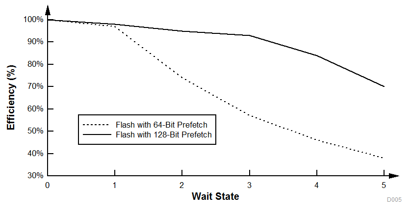
GUID-62BC42CD-C827-4B12-A92D-0EED4A398DB2-low.gifFigure 7-24 Application Code With Heavy 32-Bit Floating-Point Math Instructions
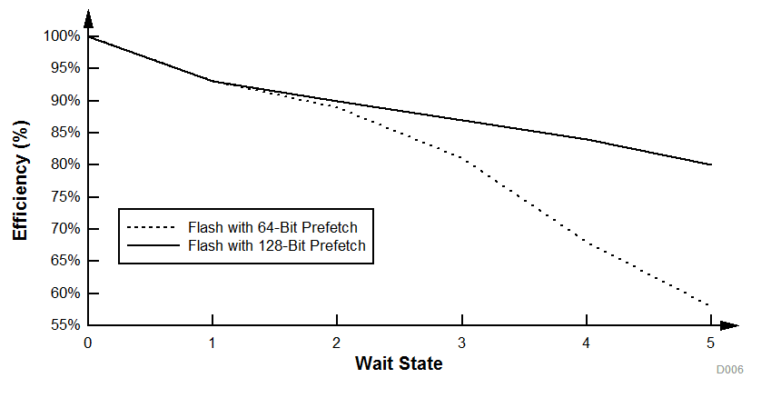
GUID-B739B7EF-303A-4840-8E86-8EA0C12E9C6F-low.gifFigure 7-25 Application Code With 16-Bit If-Else Instructions

Table 7-10 lists the Flash parameters.

Table 7-10 Flash Parameters
PARAMETER MIN TYP MAX UNIT
Program Time (1) 128 data bits + 16 ECC bits 150 300 µs
8KB sector 50 100 ms
Erase Time (2) at < 25 W/E cycles 8KB sector 15 100 ms
Erase Time (2) at 1000 W/E cycles 8KB sector 25 350 ms
Erase Time (2) at 2000 W/E cycles 8KB sector 30 600 ms
Erase Time (2) at 20K W/E cycles 8KB sector 120 4000 ms
Nwec  Write/Erase Cycles per sector 20000 cycles
Nwec Write/Erase Cycles for entire Flash (combined all sectors)(3) 100000 cycles
tretention  Data retention duration at TJ = 85oC 20 years
Program time is at the maximum device frequency.  Program time includes overhead of the flash state machine but does not include the time to transfer the following into RAM:
• Code that uses flash API to program the flash        
• Flash API itself            
• Flash data to be programmed            
In other words, the time indicated in this table is applicable after all the required code/data is available in the device RAM, ready for
programming. The transfer time will significantly vary depending on the speed of the JTAG debug probe used.
Program time calculation is based on programming 144 bits at a time at the specified operating frequency. Program time includes
Program verify by the CPU. The program time does not degrade with write/erase (W/E) cycling, but the erase time does and hence Erase time is provided for 25 W/E cycles, 1K W/E cycles, 2K W/E cycles and 20K W/E cycles.
Erase time includes Erase verify by the CPU and does not involve any data transfer.
Erase time includes Erase verify by the CPU.
Each sector, by itself, can only be erased/programmed 20,000 times. If you choose to use a sector (or multiple sectors) like an EEPROM, you can erase/program only those sectors (still limited to 20,000 cycles) without erasing/programming the entire Flash memory. Therefore, the total number of W/E cycles from a device perspective can exceed 20,000 cycles. However, even this number should not exceed 100,000 cycles.
Note:

The Main Array flash programming must be aligned to 64-bit address boundaries and each 64-bit word may only be programmed once per write/erase cycle.

The DCSM OTP programming must be aligned to 128-bit address boundaries and each 128-bit word may only be programmed once. The exceptions are:

  1. The DCSM Zx-LINKPOINTER1 and Zx-LINKPOINTER2 values in the DCSM OTP should be programmed together, and may be programmed 1 bit at a time as required by the DCSM operation.
  2. The DCSM Zx-LINKPOINTER3 values in the DCSM OTP may be programmed 1 bit at a time on a 64-bit boundary to separate it from Zx-PSWDLOCK, which must only be programmed once.