SPRS698J November   2010  – September 2021 TMS320F28062 , TMS320F28062F , TMS320F28063 , TMS320F28064 , TMS320F28065 , TMS320F28066 , TMS320F28067 , TMS320F28068F , TMS320F28068M , TMS320F28069 , TMS320F28069F , TMS320F28069M

PRODUCTION DATA  

  1. Features
  2. Applications
  3. Description
    1. 3.1 Functional Block Diagram
    2. 3.2 System Device Diagram
  4. Revision History
  5. Device Comparison
    1. 5.1 Related Products
  6. Terminal Configuration and Functions
    1. 6.1 Pin Diagrams
    2. 6.2 Signal Descriptions
      1. 6.2.1 Signal Descriptions
  7. Specifications
    1. 7.1  Absolute Maximum Ratings
    2. 7.2  ESD Ratings – Commercial
    3. 7.3  ESD Ratings – Automotive
    4. 7.4  Recommended Operating Conditions
    5. 7.5  Power Consumption Summary
      1. 7.5.1 TMS320F2806x Current Consumption at 90-MHz SYSCLKOUT
      2. 7.5.2 Reducing Current Consumption
      3. 7.5.3 Current Consumption Graphs (VREG Enabled)
    6. 7.6  Electrical Characteristics
    7. 7.7  Thermal Resistance Characteristics
      1. 7.7.1 PFP PowerPAD Package
      2. 7.7.2 PZP PowerPAD Package
      3. 7.7.3 PN Package
      4. 7.7.4 PZ Package
    8. 7.8  Thermal Design Considerations
    9. 7.9  Debug Probe Connection Without Signal Buffering for the MCU
    10. 7.10 Parameter Information
      1. 7.10.1 Timing Parameter Symbology
      2. 7.10.2 General Notes on Timing Parameters
    11. 7.11 Test Load Circuit
    12. 7.12 Power Sequencing
      1. 7.12.1 Reset ( XRS) Timing Requirements
      2. 7.12.2 Reset ( XRS) Switching Characteristics
    13. 7.13 Clock Specifications
      1. 7.13.1 Device Clock Table
        1. 7.13.1.1 2806x Clock Table and Nomenclature (90-MHz Devices)
        2. 7.13.1.2 Device Clocking Requirements/Characteristics
        3. 7.13.1.3 Internal Zero-Pin Oscillator (INTOSC1/INTOSC2) Characteristics
      2. 7.13.2 Clock Requirements and Characteristics
        1. 7.13.2.1 XCLKIN Timing Requirements – PLL Enabled
        2. 7.13.2.2 XCLKIN Timing Requirements – PLL Disabled
        3. 7.13.2.3 XCLKOUT Switching Characteristics (PLL Bypassed or Enabled)
    14. 7.14 Flash Timing
      1. 7.14.1 Flash/OTP Endurance for T Temperature Material
      2. 7.14.2 Flash/OTP Endurance for S Temperature Material
      3. 7.14.3 Flash/OTP Endurance for Q Temperature Material
      4. 7.14.4 Flash Parameters at 90-MHz SYSCLKOUT
      5. 7.14.5 Flash/OTP Access Timing
      6. 7.14.6 Flash Data Retention Duration
  8. Detailed Description
    1. 8.1 Overview
      1. 8.1.1  CPU
      2. 8.1.2  Control Law Accelerator (CLA)
      3. 8.1.3  Viterbi, Complex Math, CRC Unit (VCU)
      4. 8.1.4  Memory Bus (Harvard Bus Architecture)
      5. 8.1.5  Peripheral Bus
      6. 8.1.6  Real-Time JTAG and Analysis
      7. 8.1.7  Flash
      8. 8.1.8  M0, M1 SARAMs
      9. 8.1.9  L4 SARAM, and L0, L1, L2, L3, L5, L6, L7, and L8 DPSARAMs
      10. 8.1.10 Boot ROM
        1. 8.1.10.1 Debug Boot
        2. 8.1.10.2 GetMode
        3. 8.1.10.3 Peripheral Pins Used by the Bootloader
      11. 8.1.11 Security
      12. 8.1.12 Peripheral Interrupt Expansion (PIE) Block
      13. 8.1.13 External Interrupts (XINT1 to XINT3)
      14. 8.1.14 Internal Zero Pin Oscillators, Oscillator, and PLL
      15. 8.1.15 Watchdog
      16. 8.1.16 Peripheral Clocking
      17. 8.1.17 Low-power Modes
      18. 8.1.18 Peripheral Frames 0, 1, 2, 3 (PFn)
      19. 8.1.19 General-Purpose Input/Output (GPIO) Multiplexer
      20. 8.1.20 32-Bit CPU-Timers (0, 1, 2)
      21. 8.1.21 Control Peripherals
      22. 8.1.22 Serial Port Peripherals
    2. 8.2 Memory Maps
    3. 8.3 Register Maps
    4. 8.4 Device Debug Registers
    5. 8.5 VREG, BOR, POR
      1. 8.5.1 On-chip VREG
        1. 8.5.1.1 Using the On-chip VREG
        2. 8.5.1.2 Disabling the On-chip VREG
      2. 8.5.2 On-chip Power-On Reset (POR) and Brownout Reset (BOR) Circuit
    6. 8.6 System Control
      1. 8.6.1 Internal Zero Pin Oscillators
      2. 8.6.2 Crystal Oscillator Option
      3. 8.6.3 PLL-Based Clock Module
      4. 8.6.4 USB and HRCAP PLL Module (PLL2)
      5. 8.6.5 Loss of Input Clock (NMI Watchdog Function)
      6. 8.6.6 CPU Watchdog Module
    7. 8.7 Low-power Modes Block
    8. 8.8 Interrupts
      1. 8.8.1 External Interrupts
        1. 8.8.1.1 External Interrupt Electrical Data/Timing
          1. 8.8.1.1.1 External Interrupt Timing Requirements
          2. 8.8.1.1.2 External Interrupt Switching Characteristics
    9. 8.9 Peripherals
      1. 8.9.1  CLA Overview
      2. 8.9.2  Analog Block
        1. 8.9.2.1 Analog-to-Digital Converter (ADC)
          1. 8.9.2.1.1 Features
          2. 8.9.2.1.2 ADC Start-of-Conversion Electrical Data/Timing
            1. 8.9.2.1.2.1 External ADC Start-of-Conversion Switching Characteristics
          3. 8.9.2.1.3 On-Chip Analog-to-Digital Converter (ADC) Electrical Data/Timing
            1. 8.9.2.1.3.1 ADC Electrical Characteristics
            2. 8.9.2.1.3.2 ADC Power Modes
            3. 8.9.2.1.3.3 Internal Temperature Sensor
              1. 8.9.2.1.3.3.1 Temperature Sensor Coefficient
            4. 8.9.2.1.3.4 ADC Power-Up Control Bit Timing
              1. 8.9.2.1.3.4.1 ADC Power-Up Delays
            5. 8.9.2.1.3.5 ADC Sequential and Simultaneous Timings
        2. 8.9.2.2 ADC MUX
        3. 8.9.2.3 Comparator Block
          1. 8.9.2.3.1 On-Chip Comparator/DAC Electrical Data/Timing
            1. 8.9.2.3.1.1 Electrical Characteristics of the Comparator/DAC
      3. 8.9.3  Detailed Descriptions
      4. 8.9.4  Serial Peripheral Interface (SPI) Module
        1. 8.9.4.1 SPI Master Mode Electrical Data/Timing
          1. 8.9.4.1.1 SPI Master Mode External Timing (Clock Phase = 0)
          2. 8.9.4.1.2 SPI Master Mode External Timing (Clock Phase = 1)
        2. 8.9.4.2 SPI Slave Mode Electrical Data/Timing
          1. 8.9.4.2.1 SPI Slave Mode External Timing (Clock Phase = 0)
          2. 8.9.4.2.2 SPI Slave Mode External Timing (Clock Phase = 1)
      5. 8.9.5  Serial Communications Interface (SCI) Module
      6. 8.9.6  Multichannel Buffered Serial Port (McBSP) Module
        1. 8.9.6.1 McBSP Electrical Data/Timing
          1. 8.9.6.1.1 McBSP Transmit and Receive Timing
            1. 8.9.6.1.1.1 McBSP Timing Requirements
            2. 8.9.6.1.1.2 McBSP Switching Characteristics
          2. 8.9.6.1.2 McBSP as SPI Master or Slave Timing
            1. 8.9.6.1.2.1 McBSP as SPI Master or Slave Timing Requirements (CLKSTP = 10b, CLKXP = 0)
            2. 8.9.6.1.2.2 McBSP as SPI Master or Slave Switching Characteristics (CLKSTP = 10b, CLKXP = 0)
            3. 8.9.6.1.2.3 McBSP as SPI Master or Slave Timing Requirements (CLKSTP = 11b, CLKXP = 0)
            4. 8.9.6.1.2.4 McBSP as SPI Master or Slave Switching Characteristics (CLKSTP = 11b, CLKXP = 0)
            5. 8.9.6.1.2.5 McBSP as SPI Master or Slave Timing Requirements (CLKSTP = 10b, CLKXP = 1)
            6. 8.9.6.1.2.6 McBSP as SPI Master or Slave Switching Characteristics (CLKSTP = 10b, CLKXP = 1)
            7. 8.9.6.1.2.7 McBSP as SPI Master or Slave Timing Requirements (CLKSTP = 11b, CLKXP = 1)
            8. 8.9.6.1.2.8 McBSP as SPI Master or Slave Switching Characteristics (CLKSTP = 11b, CLKXP = 1)
      7. 8.9.7  Enhanced Controller Area Network (eCAN) Module
      8. 8.9.8  Inter-Integrated Circuit (I2C)
        1. 8.9.8.1 I2C Electrical Data/Timing
          1. 8.9.8.1.1 I2C Timing Requirements
          2. 8.9.8.1.2 I2C Switching Characteristics
      9. 8.9.9  Enhanced Pulse Width Modulator (ePWM) Modules (ePWM1 to ePWM8)
        1. 8.9.9.1 ePWM Electrical Data/Timing
          1. 8.9.9.1.1 ePWM Timing Requirements
          2. 8.9.9.1.2 ePWM Switching Characteristics
        2. 8.9.9.2 Trip-Zone Input Timing
          1. 8.9.9.2.1 Trip-Zone Input Timing Requirements
      10. 8.9.10 High-Resolution PWM (HRPWM)
        1. 8.9.10.1 HRPWM Electrical Data/Timing
          1. 8.9.10.1.1 High-Resolution PWM Characteristics
      11. 8.9.11 Enhanced Capture Module (eCAP1)
        1. 8.9.11.1 eCAP Electrical Data/Timing
          1. 8.9.11.1.1 Enhanced Capture (eCAP) Timing Requirement
          2. 8.9.11.1.2 eCAP Switching Characteristics
      12. 8.9.12 High-Resolution Capture Modules (HRCAP1 to HRCAP4)
        1. 8.9.12.1 HRCAP Electrical Data/Timing
          1. 8.9.12.1.1 High-Resolution Capture (HRCAP) Timing Requirements
      13. 8.9.13 Enhanced Quadrature Encoder Modules (eQEP1, eQEP2)
        1. 8.9.13.1 eQEP Electrical Data/Timing
          1. 8.9.13.1.1 Enhanced Quadrature Encoder Pulse (eQEP) Timing Requirements
          2. 8.9.13.1.2 eQEP Switching Characteristics
      14. 8.9.14 JTAG Port
      15. 8.9.15 General-Purpose Input/Output (GPIO) MUX
        1. 8.9.15.1 GPIO Electrical Data/Timing
          1. 8.9.15.1.1 GPIO Output Timing
            1. 8.9.15.1.1.1 General-Purpose Output Switching Characteristics
          2. 8.9.15.1.2 GPIO Input Timing
            1. 8.9.15.1.2.1 General-Purpose Input Timing Requirements
          3. 8.9.15.1.3 Sampling Window Width for Input Signals
          4. 8.9.15.1.4 Low-Power Mode Wakeup Timing
            1. 8.9.15.1.4.1 IDLE Mode Timing Requirements
            2. 8.9.15.1.4.2 IDLE Mode Switching Characteristics
            3. 8.9.15.1.4.3 STANDBY Mode Timing Requirements
            4. 8.9.15.1.4.4 STANDBY Mode Switching Characteristics
            5. 8.9.15.1.4.5 HALT Mode Timing Requirements
            6. 8.9.15.1.4.6 HALT Mode Switching Characteristics
      16. 8.9.16 Universal Serial Bus (USB)
        1. 8.9.16.1 USB Electrical Data/Timing
          1. 8.9.16.1.1 USB Input Ports DP and DM Timing Requirements
          2. 8.9.16.1.2 USB Output Ports DP and DM Switching Characteristics
  9. Applications, Implementation, and Layout
    1. 9.1 TI Reference Design
  10. 10Device and Documentation Support
    1. 10.1 Device and Development Support Tool Nomenclature
    2. 10.2 Tools and Software
    3. 10.3 Documentation Support
    4. 10.4 Support Resources
    5. 10.5 Trademarks
    6. 10.6 Electrostatic Discharge Caution
    7. 10.7 Glossary
  11. 11Mechanical, Packaging, and Orderable Information
    1. 11.1 Packaging Information

Package Options

Mechanical Data (Package|Pins)
Thermal pad, mechanical data (Package|Pins)
Orderable Information
General-Purpose Input Timing Requirements
MINMAXUNIT
tw(SP)Sampling periodQUALPRD = 01tc(SCO)cycles
QUALPRD ≠ 02tc(SCO) * QUALPRD
tw(IQSW)Input qualifier sampling windowtw(SP) * (n(1) – 1)cycles
tw(GPI) (2)Pulse duration, GPIO low/highSynchronous mode2tc(SCO)cycles
With input qualifiertw(IQSW) + tw(SP) + 1tc(SCO)
"n" represents the number of qualification samples as defined by GPxQSELn register.
For tw(GPI), pulse width is measured from VIL to VIL for an active-low signal and VIH to VIH for an active-high signal.
GUID-D9453392-8621-42B6-939F-1AF81E0CB9C7-low.gif
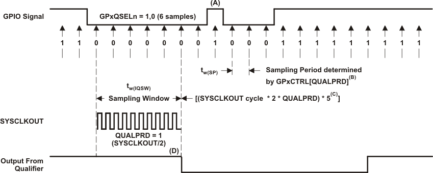
This glitch will be ignored by the input qualifier. The QUALPRD bit field specifies the qualification sampling period. The QUALPRD bit field value can vary from 00 to 0xFF. If QUALPRD = 00, then the sampling period is one SYSCLKOUT cycle. For any other value "n", the qualification sampling period in 2n SYSCLKOUT cycles (that is, at every 2n SYSCLKOUT cycles, the GPIO pin will be sampled).
The qualification period selected through the GPxCTRL register applies to groups of eight GPIO pins.
The qualification block can take either three or six samples. The GPxQSELn Register selects which sample mode is used.
In the example shown, for the qualifier to detect the change, the input should be stable for 10 SYSCLKOUT cycles or greater. In other words, the inputs should be stable for (5 × QUALPRD × 2) SYSCLKOUT cycles. This would ensure five sampling periods for detection to occur. Because external signals are driven asynchronously, an 13-SYSCLKOUT-wide pulse ensures reliable recognition.
Figure 8-57 Sampling Mode