SPRS698J November 2010 – September 2021 TMS320F28062 , TMS320F28062F , TMS320F28063 , TMS320F28064 , TMS320F28065 , TMS320F28066 , TMS320F28067 , TMS320F28068F , TMS320F28068M , TMS320F28069 , TMS320F28069F , TMS320F28069M
PRODUCTION DATA
- 1 Features
- 2 Applications
- 3 Description
- 4 Revision History
- 5 Device Comparison
- 6 Terminal Configuration and Functions
-
7 Specifications
- 7.1 Absolute Maximum Ratings
- 7.2 ESD Ratings – Commercial
- 7.3 ESD Ratings – Automotive
- 7.4 Recommended Operating Conditions
- 7.5 Power Consumption Summary
- 7.6 Electrical Characteristics
- 7.7 Thermal Resistance Characteristics
- 7.8 Thermal Design Considerations
- 7.9 Debug Probe Connection Without Signal Buffering for the MCU
- 7.10 Parameter Information
- 7.11 Test Load Circuit
- 7.12 Power Sequencing
- 7.13 Clock Specifications
- 7.14 Flash Timing
-
8 Detailed Description
- 8.1
Overview
- 8.1.1 CPU
- 8.1.2 Control Law Accelerator (CLA)
- 8.1.3 Viterbi, Complex Math, CRC Unit (VCU)
- 8.1.4 Memory Bus (Harvard Bus Architecture)
- 8.1.5 Peripheral Bus
- 8.1.6 Real-Time JTAG and Analysis
- 8.1.7 Flash
- 8.1.8 M0, M1 SARAMs
- 8.1.9 L4 SARAM, and L0, L1, L2, L3, L5, L6, L7, and L8 DPSARAMs
- 8.1.10 Boot ROM
- 8.1.11 Security
- 8.1.12 Peripheral Interrupt Expansion (PIE) Block
- 8.1.13 External Interrupts (XINT1 to XINT3)
- 8.1.14 Internal Zero Pin Oscillators, Oscillator, and PLL
- 8.1.15 Watchdog
- 8.1.16 Peripheral Clocking
- 8.1.17 Low-power Modes
- 8.1.18 Peripheral Frames 0, 1, 2, 3 (PFn)
- 8.1.19 General-Purpose Input/Output (GPIO) Multiplexer
- 8.1.20 32-Bit CPU-Timers (0, 1, 2)
- 8.1.21 Control Peripherals
- 8.1.22 Serial Port Peripherals
- 8.2 Memory Maps
- 8.3 Register Maps
- 8.4 Device Debug Registers
- 8.5 VREG, BOR, POR
- 8.6 System Control
- 8.7 Low-power Modes Block
- 8.8 Interrupts
- 8.9
Peripherals
- 8.9.1 CLA Overview
- 8.9.2 Analog Block
- 8.9.3 Detailed Descriptions
- 8.9.4 Serial Peripheral Interface (SPI) Module
- 8.9.5 Serial Communications Interface (SCI) Module
- 8.9.6
Multichannel Buffered Serial Port (McBSP) Module
- 8.9.6.1
McBSP Electrical Data/Timing
- 8.9.6.1.1 McBSP Transmit and Receive Timing
- 8.9.6.1.2
McBSP as SPI Master or Slave Timing
- 8.9.6.1.2.1 McBSP as SPI Master or Slave Timing Requirements (CLKSTP = 10b, CLKXP = 0)
- 8.9.6.1.2.2 McBSP as SPI Master or Slave Switching Characteristics (CLKSTP = 10b, CLKXP = 0)
- 8.9.6.1.2.3 McBSP as SPI Master or Slave Timing Requirements (CLKSTP = 11b, CLKXP = 0)
- 8.9.6.1.2.4 McBSP as SPI Master or Slave Switching Characteristics (CLKSTP = 11b, CLKXP = 0)
- 8.9.6.1.2.5 McBSP as SPI Master or Slave Timing Requirements (CLKSTP = 10b, CLKXP = 1)
- 8.9.6.1.2.6 McBSP as SPI Master or Slave Switching Characteristics (CLKSTP = 10b, CLKXP = 1)
- 8.9.6.1.2.7 McBSP as SPI Master or Slave Timing Requirements (CLKSTP = 11b, CLKXP = 1)
- 8.9.6.1.2.8 McBSP as SPI Master or Slave Switching Characteristics (CLKSTP = 11b, CLKXP = 1)
- 8.9.6.1
McBSP Electrical Data/Timing
- 8.9.7 Enhanced Controller Area Network (eCAN) Module
- 8.9.8 Inter-Integrated Circuit (I2C)
- 8.9.9 Enhanced Pulse Width Modulator (ePWM) Modules (ePWM1 to ePWM8)
- 8.9.10 High-Resolution PWM (HRPWM)
- 8.9.11 Enhanced Capture Module (eCAP1)
- 8.9.12 High-Resolution Capture Modules (HRCAP1 to HRCAP4)
- 8.9.13 Enhanced Quadrature Encoder Modules (eQEP1, eQEP2)
- 8.9.14 JTAG Port
- 8.9.15 General-Purpose Input/Output (GPIO) MUX
- 8.9.16 Universal Serial Bus (USB)
- 8.1
Overview
- 9 Applications, Implementation, and Layout
- 10Device and Documentation Support
- 11Mechanical, Packaging, and Orderable Information
Package Options
Mechanical Data (Package|Pins)
Thermal pad, mechanical data (Package|Pins)
Orderable Information
8.9.6 Multichannel Buffered Serial Port (McBSP) Module
The McBSP module has the following features:
- Compatible to McBSP in TMS320C28x/TMS320F28x DSP devices
- Full-duplex communication
- Double-buffered data registers that allow a continuous data stream
- Independent framing and clocking for receive and transmit
- External shift clock generation or an internal programmable frequency shift clock
- A wide selection of data sizes including 8-, 12-, 16-, 20-, 24-, or 32-bits
- 8-bit data transfers with LSB or MSB first
- Programmable polarity for both frame synchronization and data clocks
- Highly programmable internal clock and frame generation
- Direct interface to industry-standard CODECs, Analog Interface Chips (AICs), and other serially connected analog-to-digital (A/D) and digital-to-analog (D/A) devices
- Works with SPI-compatible devices
- The following application
interfaces can be supported on the McBSP:
- T1/E1 framers
- IOM-2 compliant devices
- AC97-compliant devices (the necessary multiphase frame synchronization capability is provided.)
- IIS-compliant devices
- SPI
- McBSP clock rate,
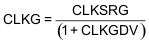
where CLKSRG source could be LSPCLK, CLKX, or CLKR. Serial port performance is limited by I/O buffer switching speed. Internal prescalers must be adjusted such that the peripheral speed is less than the I/O buffer speed limit.
See Section 8.9 for maximum I/O pin toggling speed.
On the 80-pin package, only the clock-stop mode (SPI) of the McBSP is supported.
Figure 8-38 shows the block diagram of the McBSP module.
 Figure 8-38 McBSP Module
Table 8-29 provides a summary of the McBSP registers.
| NAME | McBSP-A ADDRESS | TYPE | RESET VALUE | DESCRIPTION |
|---|---|---|---|---|
| Data Registers, Receive, Transmit | ||||
| DRR2 | 0x5000 | R | 0x0000 | McBSP Data Receive Register 2 |
| DRR1 | 0x5001 | R | 0x0000 | McBSP Data Receive Register 1 |
| DXR2 | 0x5002 | W | 0x0000 | McBSP Data Transmit Register 2 |
| DXR1 | 0x5003 | W | 0x0000 | McBSP Data Transmit Register 1 |
| McBSP Control Registers | ||||
| SPCR2 | 0x5004 | R/W | 0x0000 | McBSP Serial Port Control Register 2 |
| SPCR1 | 0x5005 | R/W | 0x0000 | McBSP Serial Port Control Register 1 |
| RCR2 | 0x5006 | R/W | 0x0000 | McBSP Receive Control Register 2 |
| RCR1 | 0x5007 | R/W | 0x0000 | McBSP Receive Control Register 1 |
| XCR2 | 0x5008 | R/W | 0x0000 | McBSP Transmit Control Register 2 |
| XCR1 | 0x5009 | R/W | 0x0000 | McBSP Transmit Control Register 1 |
| SRGR2 | 0x500A | R/W | 0x0000 | McBSP Sample Rate Generator Register 2 |
| SRGR1 | 0x500B | R/W | 0x0000 | McBSP Sample Rate Generator Register 1 |
| Multichannel Control Registers | ||||
| MCR2 | 0x500C | R/W | 0x0000 | McBSP Multichannel Register 2 |
| MCR1 | 0x500D | R/W | 0x0000 | McBSP Multichannel Register 1 |
| RCERA | 0x500E | R/W | 0x0000 | McBSP Receive Channel Enable Register Partition A |
| RCERB | 0x500F | R/W | 0x0000 | McBSP Receive Channel Enable Register Partition B |
| XCERA | 0x5010 | R/W | 0x0000 | McBSP Transmit Channel Enable Register Partition A |
| XCERB | 0x5011 | R/W | 0x0000 | McBSP Transmit Channel Enable Register Partition B |
| PCR | 0x5012 | R/W | 0x0000 | McBSP Pin Control Register |
| RCERC | 0x5013 | R/W | 0x0000 | McBSP Receive Channel Enable Register Partition C |
| RCERD | 0x5014 | R/W | 0x0000 | McBSP Receive Channel Enable Register Partition D |
| XCERC | 0x5015 | R/W | 0x0000 | McBSP Transmit Channel Enable Register Partition C |
| XCERD | 0x5016 | R/W | 0x0000 | McBSP Transmit Channel Enable Register Partition D |
| RCERE | 0x5017 | R/W | 0x0000 | McBSP Receive Channel Enable Register Partition E |
| RCERF | 0x5018 | R/W | 0x0000 | McBSP Receive Channel Enable Register Partition F |
| XCERE | 0x5019 | R/W | 0x0000 | McBSP Transmit Channel Enable Register Partition E |
| XCERF | 0x501A | R/W | 0x0000 | McBSP Transmit Channel Enable Register Partition F |
| RCERG | 0x501B | R/W | 0x0000 | McBSP Receive Channel Enable Register Partition G |
| RCERH | 0x501C | R/W | 0x0000 | McBSP Receive Channel Enable Register Partition H |
| XCERG | 0x501D | R/W | 0x0000 | McBSP Transmit Channel Enable Register Partition G |
| XCERH | 0x501E | R/W | 0x0000 | McBSP Transmit Channel Enable Register Partition H |
| MFFINT | 0x5023 | R/W | 0x0000 | McBSP Interrupt Enable Register |