SPRS439Q June 2007 – August 2022 TMS320F28232 , TMS320F28232-Q1 , TMS320F28234 , TMS320F28234-Q1 , TMS320F28235 , TMS320F28235-Q1 , TMS320F28332 , TMS320F28333 , TMS320F28334 , TMS320F28335 , TMS320F28335-Q1
PRODUCTION DATA
- 1 Features
- 2 Applications
- 3 Description
- 4 Revision History
- 5 Device Comparison
- 6 Terminal Configuration and Functions
-
7 Specifications
- 7.1 Absolute Maximum Ratings
- 7.2 ESD Ratings – Automotive
- 7.3 ESD Ratings – Commercial
- 7.4 Recommended Operating Conditions
- 7.5 Power Consumption Summary
- 7.6 Electrical Characteristics
- 7.7 Thermal Resistance Characteristics
- 7.8 Thermal Design Considerations
- 7.9
Timing and Switching Characteristics
- 7.9.1 Timing Parameter Symbology
- 7.9.2 Power Sequencing
- 7.9.3 Clock Requirements and Characteristics
- 7.9.4
Peripherals
- 7.9.4.1
General-Purpose Input/Output (GPIO)
- 7.9.4.1.1 GPIO - Output Timing
- 7.9.4.1.2 GPIO - Input Timing
- 7.9.4.1.3 Sampling Window Width for Input Signals
- 7.9.4.1.4
Low-Power Mode Wakeup Timing
- 7.9.4.1.4.1 IDLE Mode Timing Requirements
- 7.9.4.1.4.2 IDLE Mode Switching Characteristics
- 7.9.4.1.4.3 IDLE Mode Timing Diagram
- 7.9.4.1.4.4 STANDBY Mode Timing Requirements
- 7.9.4.1.4.5 STANDBY Mode Switching Characteristics
- 7.9.4.1.4.6 STANDBY Mode Timing Diagram
- 7.9.4.1.4.7 HALT Mode Timing Requirements
- 7.9.4.1.4.8 HALT Mode Switching Characteristics
- 7.9.4.1.4.9 HALT Mode Timing Diagram
- 7.9.4.2 Enhanced Control Peripherals
- 7.9.4.3 External Interrupt Timing
- 7.9.4.4 I2C Electrical Specification and Timing
- 7.9.4.5 Serial Peripheral Interface (SPI) Timing
- 7.9.4.6
Multichannel Buffered Serial Port (McBSP) Timing
- 7.9.4.6.1 McBSP Transmit and Receive Timing
- 7.9.4.6.2
McBSP as SPI Master or Slave Timing
- 7.9.4.6.2.1 McBSP as SPI Master or Slave Timing Requirements (CLKSTP = 10b, CLKXP = 0)
- 7.9.4.6.2.2 McBSP as SPI Master or Slave Switching Characteristics (CLKSTP = 10b, CLKXP = 0)
- 7.9.4.6.2.3 McBSP as SPI Master or Slave Timing Requirements (CLKSTP = 11b, CLKXP = 0)
- 7.9.4.6.2.4 McBSP as SPI Master or Slave Switching Characteristics (CLKSTP = 11b, CLKXP = 0)
- 7.9.4.6.2.5 McBSP as SPI Master or Slave Timing Requirements (CLKSTP = 10b, CLKXP = 1)
- 7.9.4.6.2.6 McBSP as SPI Master or Slave Switching Characteristics (CLKSTP = 10b, CLKXP = 1)
- 7.9.4.6.2.7 McBSP as SPI Master or Slave Timing Requirements (CLKSTP = 11b, CLKXP = 1)
- 7.9.4.6.2.8 McBSP as SPI Master or Slave Switching Characteristics (CLKSTP = 11b, CLKXP = 1)
- 7.9.4.1
General-Purpose Input/Output (GPIO)
- 7.9.5 JTAG Debug Probe Connection Without Signal Buffering for the MCU
- 7.9.6
External Interface (XINTF) Timing
- 7.9.6.1 USEREADY = 0
- 7.9.6.2 Synchronous Mode (USEREADY = 1, READYMODE = 0)
- 7.9.6.3 Asynchronous Mode (USEREADY = 1, READYMODE = 1)
- 7.9.6.4 XINTF Signal Alignment to XCLKOUT
- 7.9.6.5 External Interface Read Timing
- 7.9.6.6 External Interface Write Timing
- 7.9.6.7
External Interface Ready-on-Read Timing With One External Wait State
- 7.9.6.7.1 External Interface Read Switching Characteristics (Ready-on-Read, One Wait State)
- 7.9.6.7.2 External Interface Read Timing Requirements (Ready-on-Read, One Wait State)
- 7.9.6.7.3 Synchronous XREADY Timing Requirements (Ready-on-Read, One Wait State)
- 7.9.6.7.4 Asynchronous XREADY Timing Requirements (Ready-on-Read, One Wait State)
- 7.9.6.8 External Interface Ready-on-Write Timing With One External Wait State
- 7.9.6.9 XHOLD and XHOLDA Timing
- 7.9.7 Flash Timing
- 7.10 On-Chip Analog-to-Digital Converter
- 7.11 Migrating Between F2833x Devices and F2823x Devices
-
8 Detailed Description
- 8.1
Brief Descriptions
- 8.1.1 C28x CPU
- 8.1.2 Memory Bus (Harvard Bus Architecture)
- 8.1.3 Peripheral Bus
- 8.1.4 Real-Time JTAG and Analysis
- 8.1.5 External Interface (XINTF)
- 8.1.6 Flash
- 8.1.7 M0, M1 SARAMs
- 8.1.8 L0, L1, L2, L3, L4, L5, L6, L7 SARAMs
- 8.1.9 Boot ROM
- 8.1.10 Security
- 8.1.11 Peripheral Interrupt Expansion (PIE) Block
- 8.1.12 External Interrupts (XINT1–XINT7, XNMI)
- 8.1.13 Oscillator and PLL
- 8.1.14 Watchdog
- 8.1.15 Peripheral Clocking
- 8.1.16 Low-Power Modes
- 8.1.17 Peripheral Frames 0, 1, 2, 3 (PFn)
- 8.1.18 General-Purpose Input/Output (GPIO) Multiplexer
- 8.1.19 32-Bit CPU-Timers (0, 1, 2)
- 8.1.20 Control Peripherals
- 8.1.21 Serial Port Peripherals
- 8.2
Peripherals
- 8.2.1 DMA Overview
- 8.2.2 32-Bit CPU-Timer 0, CPU-Timer 1, CPU-Timer 2
- 8.2.3 Enhanced PWM Modules
- 8.2.4 High-Resolution PWM (HRPWM)
- 8.2.5 Enhanced CAP Modules
- 8.2.6 Enhanced QEP Modules
- 8.2.7 Analog-to-Digital Converter (ADC) Module
- 8.2.8 Multichannel Buffered Serial Port (McBSP) Module
- 8.2.9 Enhanced Controller Area Network (eCAN) Modules (eCAN-A and eCAN-B)
- 8.2.10 Serial Communications Interface (SCI) Modules (SCI-A, SCI-B, SCI-C)
- 8.2.11 Serial Peripheral Interface (SPI) Module (SPI-A)
- 8.2.12 Inter-Integrated Circuit (I2C)
- 8.2.13 GPIO MUX
- 8.2.14 External Interface (XINTF)
- 8.3 Memory Maps
- 8.4 Register Map
- 8.5 Interrupts
- 8.6 System Control
- 8.7 Low-Power Modes Block
- 8.1
Brief Descriptions
- 9 Applications, Implementation, and Layout
- 10Device and Documentation Support
- 11Mechanical, Packaging, and Orderable Information
Package Options
Refer to the PDF data sheet for device specific package drawings
Mechanical Data (Package|Pins)
- PGF|176
- PTP|176
Thermal pad, mechanical data (Package|Pins)
- PTP|176
Orderable Information
8.2.10 Serial Communications Interface (SCI) Modules (SCI-A, SCI-B, SCI-C)
The devices include three serial communications interface (SCI) modules. The SCI modules support digital communications between the CPU and other asynchronous peripherals that use the standard nonreturn-to-zero (NRZ) format. The SCI receiver and transmitter are double-buffered, and each has its own separate enable and interrupt bits. Both can be operated independently or simultaneously in the full-duplex mode. To ensure data integrity, the SCI checks received data for break detection, parity, overrun, and framing errors. The bit rate is programmable to more than 65000 different speeds through a 16-bit baud-select register.
Features of each SCI module include:
- Two external pins:
- SCITXD: SCI transmit-output pin
- SCIRXD: SCI receive-input
pin Note: Both pins can be used as GPIO if not used for SCI.
- Baud rate programmable to 64K different rates:
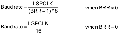 Note:
Note:See Section 7 for maximum I/O pin toggling speed.
- Data-word format
- One start bit
- Data-word length programmable from one to eight bits
- Optional even/odd/no parity bit
- One or two stop bits
- Four error-detection flags: parity, overrun, framing, and break detection
- Two wake-up multiprocessor modes: idle-line and address bit
- Half- or full-duplex operation
- Double-buffered receive and transmit functions
- Transmitter and receiver
operations can be accomplished through interrupt-driven or polled algorithms
with status flags.
- Transmitter: TXRDY flag (transmitter-buffer register is ready to receive another character) and TX EMPTY flag (transmitter-shift register is empty)
- Receiver: RXRDY flag (receiver-buffer register is ready to receive another character), BRKDT flag (break condition occurred), and RX ERROR flag (monitoring four interrupt conditions)
- Separate enable bits for transmitter and receiver interrupts (except BRKDT)
- NRZ (nonreturn-to-zero) format
All registers in this module are 8-bit registers that are connected to Peripheral Frame 2. When a register is accessed, the register data is in the lower byte (7-0), and the upper byte (15-8) is read as zeros. Writing to the upper byte has no effect.
Enhanced features:
- Auto baud-detect hardware logic
- 16-level transmit/receive FIFO
The SCI port operation is configured and controlled by the registers listed in Table 8-12, Table 8-13, and Table 8-14.
| NAME(1) | ADDRESS | SIZE (x16) | DESCRIPTION |
|---|---|---|---|
| SCICCRA | 0x7050 | 1 | SCI-A Communications Control Register |
| SCICTL1A | 0x7051 | 1 | SCI-A Control Register 1 |
| SCIHBAUDA | 0x7052 | 1 | SCI-A Baud Register, High Bits |
| SCILBAUDA | 0x7053 | 1 | SCI-A Baud Register, Low Bits |
| SCICTL2A | 0x7054 | 1 | SCI-A Control Register 2 |
| SCIRXSTA | 0x7055 | 1 | SCI-A Receive Status Register |
| SCIRXEMUA | 0x7056 | 1 | SCI-A Receive Emulation Data Buffer Register |
| SCIRXBUFA | 0x7057 | 1 | SCI-A Receive Data Buffer Register |
| SCITXBUFA | 0x7059 | 1 | SCI-A Transmit Data Buffer Register |
| SCIFFTXA(2) | 0x705A | 1 | SCI-A FIFO Transmit Register |
| SCIFFRXA(2) | 0x705B | 1 | SCI-A FIFO Receive Register |
| SCIFFCTA(2) | 0x705C | 1 | SCI-A FIFO Control Register |
| SCIPRIA | 0x705F | 1 | SCI-A Priority Control Register |
| NAME(1) | ADDRESS | SIZE (x16) | DESCRIPTION |
|---|---|---|---|
| SCICCRB | 0x7750 | 1 | SCI-B Communications Control Register |
| SCICTL1B | 0x7751 | 1 | SCI-B Control Register 1 |
| SCIHBAUDB | 0x7752 | 1 | SCI-B Baud Register, High Bits |
| SCILBAUDB | 0x7753 | 1 | SCI-B Baud Register, Low Bits |
| SCICTL2B | 0x7754 | 1 | SCI-B Control Register 2 |
| SCIRXSTB | 0x7755 | 1 | SCI-B Receive Status Register |
| SCIRXEMUB | 0x7756 | 1 | SCI-B Receive Emulation Data Buffer Register |
| SCIRXBUFB | 0x7757 | 1 | SCI-B Receive Data Buffer Register |
| SCITXBUFB | 0x7759 | 1 | SCI-B Transmit Data Buffer Register |
| SCIFFTXB(2) | 0x775A | 1 | SCI-B FIFO Transmit Register |
| SCIFFRXB(2) | 0x775B | 1 | SCI-B FIFO Receive Register |
| SCIFFCTB(2) | 0x775C | 1 | SCI-B FIFO Control Register |
| SCIPRIB | 0x775F | 1 | SCI-B Priority Control Register |
| NAME(1) | ADDRESS | SIZE (x16) | DESCRIPTION |
|---|---|---|---|
| SCICCRC | 0x7770 | 1 | SCI-C Communications Control Register |
| SCICTL1C | 0x7771 | 1 | SCI-C Control Register 1 |
| SCIHBAUDC | 0x7772 | 1 | SCI-C Baud Register, High Bits |
| SCILBAUDC | 0x7773 | 1 | SCI-C Baud Register, Low Bits |
| SCICTL2C | 0x7774 | 1 | SCI-C Control Register 2 |
| SCIRXSTC | 0x7775 | 1 | SCI-C Receive Status Register |
| SCIRXEMUC | 0x7776 | 1 | SCI-C Receive Emulation Data Buffer Register |
| SCIRXBUFC | 0x7777 | 1 | SCI-C Receive Data Buffer Register |
| SCITXBUFC | 0x7779 | 1 | SCI-C Transmit Data Buffer Register |
| SCIFFTXC(2) | 0x777A | 1 | SCI-C FIFO Transmit Register |
| SCIFFRXC(2) | 0x777B | 1 | SCI-C FIFO Receive Register |
| SCIFFCTC(2) | 0x777C | 1 | SCI-C FIFO Control Register |
| SCIPRC | 0x777F | 1 | SCI-C Priority Control Register |
Figure 8-15 shows the SCI module block diagram.
 Module Block Diagram") Figure 8-15 Serial
Communications Interface (SCI) Module Block Diagram
Figure 8-15 Serial
Communications Interface (SCI) Module Block Diagram