SPRS439Q June 2007 – August 2022 TMS320F28232 , TMS320F28232-Q1 , TMS320F28234 , TMS320F28234-Q1 , TMS320F28235 , TMS320F28235-Q1 , TMS320F28332 , TMS320F28333 , TMS320F28334 , TMS320F28335 , TMS320F28335-Q1
PRODUCTION DATA
- 1 Features
- 2 Applications
- 3 Description
- 4 Revision History
- 5 Device Comparison
- 6 Terminal Configuration and Functions
-
7 Specifications
- 7.1 Absolute Maximum Ratings
- 7.2 ESD Ratings – Automotive
- 7.3 ESD Ratings – Commercial
- 7.4 Recommended Operating Conditions
- 7.5 Power Consumption Summary
- 7.6 Electrical Characteristics
- 7.7 Thermal Resistance Characteristics
- 7.8 Thermal Design Considerations
- 7.9
Timing and Switching Characteristics
- 7.9.1 Timing Parameter Symbology
- 7.9.2 Power Sequencing
- 7.9.3 Clock Requirements and Characteristics
- 7.9.4
Peripherals
- 7.9.4.1
General-Purpose Input/Output (GPIO)
- 7.9.4.1.1 GPIO - Output Timing
- 7.9.4.1.2 GPIO - Input Timing
- 7.9.4.1.3 Sampling Window Width for Input Signals
- 7.9.4.1.4
Low-Power Mode Wakeup Timing
- 7.9.4.1.4.1 IDLE Mode Timing Requirements
- 7.9.4.1.4.2 IDLE Mode Switching Characteristics
- 7.9.4.1.4.3 IDLE Mode Timing Diagram
- 7.9.4.1.4.4 STANDBY Mode Timing Requirements
- 7.9.4.1.4.5 STANDBY Mode Switching Characteristics
- 7.9.4.1.4.6 STANDBY Mode Timing Diagram
- 7.9.4.1.4.7 HALT Mode Timing Requirements
- 7.9.4.1.4.8 HALT Mode Switching Characteristics
- 7.9.4.1.4.9 HALT Mode Timing Diagram
- 7.9.4.2 Enhanced Control Peripherals
- 7.9.4.3 External Interrupt Timing
- 7.9.4.4 I2C Electrical Specification and Timing
- 7.9.4.5 Serial Peripheral Interface (SPI) Timing
- 7.9.4.6
Multichannel Buffered Serial Port (McBSP) Timing
- 7.9.4.6.1 McBSP Transmit and Receive Timing
- 7.9.4.6.2
McBSP as SPI Master or Slave Timing
- 7.9.4.6.2.1 McBSP as SPI Master or Slave Timing Requirements (CLKSTP = 10b, CLKXP = 0)
- 7.9.4.6.2.2 McBSP as SPI Master or Slave Switching Characteristics (CLKSTP = 10b, CLKXP = 0)
- 7.9.4.6.2.3 McBSP as SPI Master or Slave Timing Requirements (CLKSTP = 11b, CLKXP = 0)
- 7.9.4.6.2.4 McBSP as SPI Master or Slave Switching Characteristics (CLKSTP = 11b, CLKXP = 0)
- 7.9.4.6.2.5 McBSP as SPI Master or Slave Timing Requirements (CLKSTP = 10b, CLKXP = 1)
- 7.9.4.6.2.6 McBSP as SPI Master or Slave Switching Characteristics (CLKSTP = 10b, CLKXP = 1)
- 7.9.4.6.2.7 McBSP as SPI Master or Slave Timing Requirements (CLKSTP = 11b, CLKXP = 1)
- 7.9.4.6.2.8 McBSP as SPI Master or Slave Switching Characteristics (CLKSTP = 11b, CLKXP = 1)
- 7.9.4.1
General-Purpose Input/Output (GPIO)
- 7.9.5 JTAG Debug Probe Connection Without Signal Buffering for the MCU
- 7.9.6
External Interface (XINTF) Timing
- 7.9.6.1 USEREADY = 0
- 7.9.6.2 Synchronous Mode (USEREADY = 1, READYMODE = 0)
- 7.9.6.3 Asynchronous Mode (USEREADY = 1, READYMODE = 1)
- 7.9.6.4 XINTF Signal Alignment to XCLKOUT
- 7.9.6.5 External Interface Read Timing
- 7.9.6.6 External Interface Write Timing
- 7.9.6.7
External Interface Ready-on-Read Timing With One External Wait State
- 7.9.6.7.1 External Interface Read Switching Characteristics (Ready-on-Read, One Wait State)
- 7.9.6.7.2 External Interface Read Timing Requirements (Ready-on-Read, One Wait State)
- 7.9.6.7.3 Synchronous XREADY Timing Requirements (Ready-on-Read, One Wait State)
- 7.9.6.7.4 Asynchronous XREADY Timing Requirements (Ready-on-Read, One Wait State)
- 7.9.6.8 External Interface Ready-on-Write Timing With One External Wait State
- 7.9.6.9 XHOLD and XHOLDA Timing
- 7.9.7 Flash Timing
- 7.10 On-Chip Analog-to-Digital Converter
- 7.11 Migrating Between F2833x Devices and F2823x Devices
-
8 Detailed Description
- 8.1
Brief Descriptions
- 8.1.1 C28x CPU
- 8.1.2 Memory Bus (Harvard Bus Architecture)
- 8.1.3 Peripheral Bus
- 8.1.4 Real-Time JTAG and Analysis
- 8.1.5 External Interface (XINTF)
- 8.1.6 Flash
- 8.1.7 M0, M1 SARAMs
- 8.1.8 L0, L1, L2, L3, L4, L5, L6, L7 SARAMs
- 8.1.9 Boot ROM
- 8.1.10 Security
- 8.1.11 Peripheral Interrupt Expansion (PIE) Block
- 8.1.12 External Interrupts (XINT1–XINT7, XNMI)
- 8.1.13 Oscillator and PLL
- 8.1.14 Watchdog
- 8.1.15 Peripheral Clocking
- 8.1.16 Low-Power Modes
- 8.1.17 Peripheral Frames 0, 1, 2, 3 (PFn)
- 8.1.18 General-Purpose Input/Output (GPIO) Multiplexer
- 8.1.19 32-Bit CPU-Timers (0, 1, 2)
- 8.1.20 Control Peripherals
- 8.1.21 Serial Port Peripherals
- 8.2
Peripherals
- 8.2.1 DMA Overview
- 8.2.2 32-Bit CPU-Timer 0, CPU-Timer 1, CPU-Timer 2
- 8.2.3 Enhanced PWM Modules
- 8.2.4 High-Resolution PWM (HRPWM)
- 8.2.5 Enhanced CAP Modules
- 8.2.6 Enhanced QEP Modules
- 8.2.7 Analog-to-Digital Converter (ADC) Module
- 8.2.8 Multichannel Buffered Serial Port (McBSP) Module
- 8.2.9 Enhanced Controller Area Network (eCAN) Modules (eCAN-A and eCAN-B)
- 8.2.10 Serial Communications Interface (SCI) Modules (SCI-A, SCI-B, SCI-C)
- 8.2.11 Serial Peripheral Interface (SPI) Module (SPI-A)
- 8.2.12 Inter-Integrated Circuit (I2C)
- 8.2.13 GPIO MUX
- 8.2.14 External Interface (XINTF)
- 8.3 Memory Maps
- 8.4 Register Map
- 8.5 Interrupts
- 8.6 System Control
- 8.7 Low-Power Modes Block
- 8.1
Brief Descriptions
- 9 Applications, Implementation, and Layout
- 10Device and Documentation Support
- 11Mechanical, Packaging, and Orderable Information
Package Options
Refer to the PDF data sheet for device specific package drawings
Mechanical Data (Package|Pins)
- PGF|176
Thermal pad, mechanical data (Package|Pins)
Orderable Information
8.2.7 Analog-to-Digital Converter (ADC) Module
A simplified functional block diagram of the ADC module is shown in Figure 8-8. The ADC module consists of a 12-bit ADC with a built-in sample-and-hold (S/H) circuit. Functions of the ADC module include:
- 12-bit ADC core with built-in S/H
- Analog input: 0.0 V to 3.0 V (Voltages above 3.0 V produce full-scale conversion results.)
- Fast conversion rate: Up to 80 ns at 25-MHz ADC clock, 12.5 MSPS
- 16 dedicated ADC channels. 8 channels multiplexed per Sample/Hold
- Autosequencing capability provides up to 16 "autoconversions" in a single session. Each conversion can be programmed to select any 1 of 16 input channels
- Sequencer can be operated as two independent 8-state sequencers or as one large 16-state sequencer (that is, two cascaded 8-state sequencers)
- Sixteen result registers (individually addressable) to store conversion values
- The digital value of the input analog voltage is derived by:
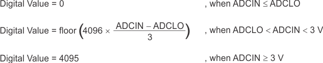
- The digital value of the input analog voltage is derived by:
- Multiple triggers as sources for the start-of-conversion (SOC) sequence
- S/W - software immediate start
- ePWM start of conversion
- XINT2 ADC start of conversion
- Flexible interrupt control allows interrupt request on every end-of-sequence (EOS) or every other EOS.
- Sequencer can operate in "start/stop" mode, allowing multiple "time-sequenced triggers" to synchronize conversions.
- SOCA and SOCB triggers can operate independently in dual-sequencer mode.
- Sample-and-hold (S/H) acquisition time window has separate prescale control.
The ADC module in the 2833x/2823x devices has been enhanced to provide flexible interface to ePWM peripherals. The ADC interface is built around a fast, 12-bit ADC module with a fast conversion rate of up to 80 ns at 25-MHz ADC clock. The ADC module has 16 channels, configurable as two independent 8-channel modules. The two independent 8-channel modules can be cascaded to form a 16-channel module. Although there are multiple input channels and two sequencers, there is only one converter in the ADC module. Figure 8-8 shows the block diagram of the ADC module.
The two 8-channel modules have the capability to autosequence a series of conversions, each module has the choice of selecting any one of the respective eight channels available through an analog MUX. In the cascaded mode, the autosequencer functions as a single 16-channel sequencer. On each sequencer, once the conversion is complete, the selected channel value is stored in its respective RESULT register. Autosequencing allows the system to convert the same channel multiple times, allowing the user to perform oversampling algorithms. This gives increased resolution over traditional single-sampled conversion results.
 Figure 8-8 Block Diagram of the ADC Module
To obtain the specified accuracy of the ADC, proper board layout is very critical. To the best extent possible, traces leading to the ADCIN pins should not run in close proximity to the digital signal paths. This is to minimize switching noise on the digital lines from getting coupled to the ADC inputs. Furthermore, proper isolation techniques must be used to isolate the ADC module power pins ( VDD1A18, VDD2A18 , VDDA2, VDDAIO) from the digital supply.Figure 8-9 shows the ADC pin connections for the devices.
- The ADC registers are accessed at the SYSCLKOUT rate. The internal timing of the ADC module is controlled by the high-speed peripheral clock (HSPCLK).
- The behavior of the ADC module based on the state of the ADCENCLK and HALT signals is as follows:
- ADCENCLK: On reset, this signal will be low. While reset is active-low ( XRS) the clock to the register will still function. This is necessary to make sure all registers and modes go into their default reset state. The analog module, however, will be in a low-power inactive state. As soon as reset goes high, then the clock to the registers will be disabled. When the user sets the ADCENCLK signal high, then the clocks to the registers will be enabled and the analog module will be enabled. There will be a certain time delay (ms range) before the ADC is stable and can be used.
- HALT: This mode only affects the analog module. It does not affect the registers. In this mode, the ADC module goes into low-power mode. This mode also will stop the clock to the CPU, which will stop the HSPCLK; therefore, the ADC register logic will be turned off indirectly.
Figure 8-9 shows the ADC pin-biasing for internal reference and Figure 8-10 shows the ADC pin-biasing for external reference.


The temperature rating of any recommended component must match the rating of the end product.