SCDS384B September 2018 – August 2025 TMUX6119
PRODUCTION DATA
- 1
- 1 Features
- 2 Applications
- 3 Description
- 4 Pin Configuration and Functions
-
5 Specifications
- 5.1 Absolute Maximum Ratings
- 5.2 ESD Ratings
- 5.3 Thermal Information
- 5.4 Recommended Operating Conditions
- 5.5 Electrical Characteristics (Dual Supplies: ±15V)
- 5.6 Switching Characteristics (Dual Supplies: ±15V)
- 5.7 Electrical Characteristics (Single Supply: 12V)
- 5.8 Switching Characteristics (Single Supply: 12V)
- 5.9 Typical Characteristics
- 6 Parameter Measurement Information
-
7 Detailed Description
- 7.1
Overview
- 7.1.1 On-Resistance
- 7.1.2 Off-Leakage Current
- 7.1.3 On-Leakage Current
- 7.1.4 Transition Time
- 7.1.5 Break-Before-Make Delay
- 7.1.6 Enable Turn-On and Enable Turn-Off Time
- 7.1.7 Charge Injection
- 7.1.8 Off Isolation
- 7.1.9 Channel-to-Channel Crosstalk
- 7.1.10 Bandwidth
- 7.1.11 THD + Noise
- 7.1.12 AC Power Supply Rejection Ratio (AC PSRR)
- 7.2 Functional Block Diagram
- 7.3 Feature Description
- 7.4 Device Functional Modes
- 7.1
Overview
- 8 Application and Implementation
- 9 Power Supply Recommendations
- 10Layout
- 11Device and Documentation Support
- 12Revision History
- 13Mechanical, Packaging, and Orderable Information
Package Options
Mechanical Data (Package|Pins)
- DCN|8
Thermal pad, mechanical data (Package|Pins)
Orderable Information
7.3.2 Ultra-low Charge Injection
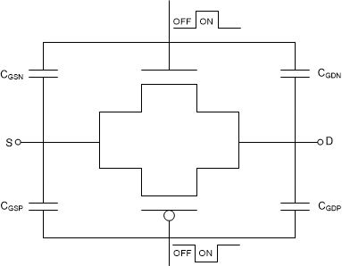
The TMUX6119 is implemented with simple transmission gate topology, as shown in Figure 7-15. Any mismatch in the stray capacitance associated with the NMOS and PMOS causes an output level change whenever the switch is opened or closed.
 Figure 7-15 Transmission Gate Topology
The TMUX6119 utilizes special charge-injection cancellation circuitry that reduces the source (SA or SB)-to-drain (D) charge injection to as low as 0.19pC at VS = 0V, as shown in Figure 7-16.
 Figure 7-16 Charge Injection vs Source Voltage
The drain (D)-to-source (SA or SB) charge injection becomes important when the device is used as a demultiplexer (demux), where D becomes the input and Sx becomes the output. Figure 7-17 shows the drain-to-source charge injection across the full signal range.
 Figure 7-17 Charge Injection vs Drain Voltage