SCDS397B November 2018 – August 2025 TMUX6136
PRODUCTION DATA
- 1
- 1 Features
- 2 Applications
- 3 Description
- 4 Pin Configuration and Functions
-
5 Specifications
- 5.1 Absolute Maximum Ratings
- 5.2 ESD Ratings
- 5.3 Thermal Information
- 5.4 Recommended Operating Conditions
- 5.5 Electrical Characteristics (Dual Supplies: ±15V)
- 5.6 Switching Characteristics (Dual Supplies: ±15V)
- 5.7 Electrical Characteristics (Single Supply: 12V)
- 5.8 Switching Characteristics (Single Supply: 12V)
- 5.9 Typical Characteristics
- 6 Detailed Description
- 7 Application and Implementation
- 8 Power Supply Recommendations
- 9 Layout
- 10Device and Documentation Support
- 11Revision History
- 12Mechanical, Packaging, and Orderable Information
Package Options
Mechanical Data (Package|Pins)
- PW|16
Thermal pad, mechanical data (Package|Pins)
Orderable Information
7.2.3 Application Curve
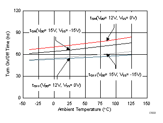
The fast transition time of the TMUX6136 and low input or output parasitic capacitance help minimize the settling time, making the TMUX6136 an excellent candidate to implement the FVMC and FCMV functions of the PMU. Figure 6-10 shows the plot for the transition time versus temperature for the TMUX6136.
 Figure 7-5 Transition Time vs Temperature for
TMUX6136