SCDS419D November 2020 – January 2022 TMUX6208 , TMUX6209
PRODUCTION DATA
- 1 Features
- 2 Applications
- 3 Description
- 4 Revision History
- 5 Device Comparison Table
- 6 Pin Configuration and Functions
-
7 Specifications
- 7.1 Absolute Maximum Ratings
- 7.2 ESD Ratings
- 7.3 Thermal Information
- 7.4 Recommended Operating Conditions
- 7.5 Source or Drain Continuous Current
- 7.6 ±15 V Dual Supply: Electrical Characteristics
- 7.7 ±15 V Dual Supply: Switching Characteristics
- 7.8 36 V Single Supply: Electrical Characteristics
- 7.9 36 V Single Supply: Switching Characteristics
- 7.10 12 V Single Supply: Electrical Characteristics
- 7.11 12 V Single Supply: Switching Characteristics
- 7.12 ±5 V Dual Supply: Electrical Characteristics
- 7.13 ±5 V Dual Supply: Switching Characteristics
- 7.14 Typical Characteristics
-
8 Parameter Measurement Information
- 8.1 On-Resistance
- 8.2 Off-Leakage Current
- 8.3 On-Leakage Current
- 8.4 Transition Time
- 8.5 tON(EN) and tOFF(EN)
- 8.6 Break-Before-Make
- 8.7 tON (VDD) Time
- 8.8 Propagation Delay
- 8.9 Charge Injection
- 8.10 Off Isolation
- 8.11 Crosstalk
- 8.12 Bandwidth
- 8.13 THD + Noise
- 8.14 Power Supply Rejection Ratio (PSRR)
- 9 Detailed Description
- 10Application and Implementation
- 11Power Supply Recommendations
- 12Layout
- 13Device and Documentation Support
- 14Mechanical, Packaging, and Orderable Information
Package Options
Mechanical Data (Package|Pins)
Thermal pad, mechanical data (Package|Pins)
- RUM|16
Orderable Information
10.2 Typical Application
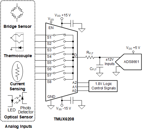
One example to take advantage of TMUX6208 performance is the implementation of multiplexed data aquisition front end for multiple input sensors. Applications such as analog input modules for programmable logic controllers (PLCs), data aquisition (DAQ), and seminconducter test systems commonly need to monitor multiple signals into a single ADC channel. The multiple inputs can come from different system voltages being montitored, or environemental sensors such as temperature or humidity. Figure 9-1 shows a simplified example of monitoring multiple inputs into a single ADC using a multiplexer.
 Figure 10-1 Multiplexed Data Aqcuisition Front End.