SCDS403C february 2021 – july 2023 TMUX7308F , TMUX7309F
PRODUCTION DATA
- 1
- 1 Features
- 2 Applications
- 3 Description
- 4 Revision History
- 5 Device Comparison Table
- 6 Pin Configuration and Functions
-
7 Specifications
- 7.1 Absolute Maximum Ratings
- 7.2 ESD Ratings
- 7.3 Thermal Information
- 7.4 Recommended Operating Conditions
- 7.5 Electrical Characteristics (Global)
- 7.6 ±15 V Dual Supply: Electrical Characteristics
- 7.7 ±20 V Dual Supply: Electrical Characteristics
- 7.8 12 V Single Supply: Electrical Characteristics
- 7.9 36 V Single Supply: Electrical Characteristics
- 7.10 Typical Characteristics
-
8 Parameter Measurement Information
- 8.1 On-Resistance
- 8.2 Off-Leakage Current
- 8.3 On-Leakage Current
- 8.4 Input and Output Leakage Current Under Overvoltage Fault
- 8.5 Break-Before-Make Delay
- 8.6 Enable Delay Time
- 8.7 Transition Time
- 8.8 Fault Response Time
- 8.9 Fault Recovery Time
- 8.10 Charge Injection
- 8.11 Off Isolation
- 8.12 Crosstalk
- 8.13 Bandwidth
- 8.14 THD + Noise
- 9 Detailed Description
- 10Application and Implementation
- 11Device and Documentation Support
- 12Mechanical, Packaging, and Orderable Information
Package Options
Mechanical Data (Package|Pins)
Thermal pad, mechanical data (Package|Pins)
Orderable Information
8.14 THD + Noise
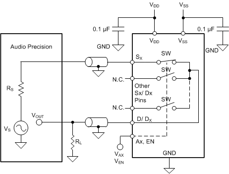
The total harmonic distortion (THD) of a signal is a measurement of the harmonic distortion, and is defined as the ratio of the sum of the powers of all harmonic components to the power of the fundamental frequency at the multiplexer output. The on-resistance of the TMUX7308F and TMUX7309F varies with the amplitude of the input signal and results in distortion when the drain pin is connected to a low-impedance load. Total harmonic distortion plus noise is denoted as THD+N. Figure 8-16 shows the setup used to measure THD+N of the devices.
 Figure 8-16 THD+N Measurement
Setup