SCDS400B march 2022 – july 2023 TMUX7348F , TMUX7349F
PRODMIX
- 1
- 1 Features
- 2 Applications
- 3 Description
- 4 Revision History
- 5 Device Comparison Table
- 6 Pin Configuration and Functions
-
7 Specifications
- 7.1 Absolute Maximum Ratings
- 7.2 ESD Ratings
- 7.3 Thermal Information
- 7.4 Recommended Operating Conditions
- 7.5 Electrical Characteristics (Global)
- 7.6 ±15 V Dual Supply: Electrical Characteristics
- 7.7 ±20 V Dual Supply: Electrical Characteristics
- 7.8 12 V Single Supply: Electrical Characteristics
- 7.9 36 V Single Supply: Electrical Characteristics
- 7.10 Typical Characteristics
-
8 Parameter Measurement Information
- 8.1 On-Resistance
- 8.2 Off-Leakage Current
- 8.3 On-Leakage Current
- 8.4 Input and Output Leakage Current Under Overvoltage Fault
- 8.5 Break-Before-Make Delay
- 8.6 Enable Delay Time
- 8.7 Transition Time
- 8.8 Fault Response Time
- 8.9 Fault Recovery Time
- 8.10 Fault Flag Response Time
- 8.11 Fault Flag Recovery Time
- 8.12 Charge Injection
- 8.13 Off Isolation
- 8.14 Crosstalk
- 8.15 Bandwidth
- 8.16 THD + Noise
-
9 Detailed Description
- 9.1 Overview
- 9.2 Functional Block Diagram
- 9.3 Feature Description
- 9.4 Device Functional Modes
- 10Application and Implementation
- 11Device and Documentation Support
- 12Mechanical, Packaging, and Orderable Information
Package Options
Mechanical Data (Package|Pins)
Thermal pad, mechanical data (Package|Pins)
Orderable Information
6 Pin Configuration and Functions
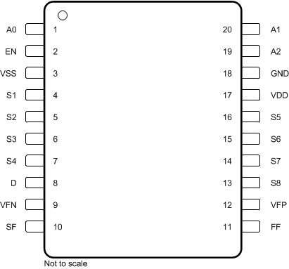
 Figure 6-1 PW Package, 20-Pin TSSOP
(Top View)
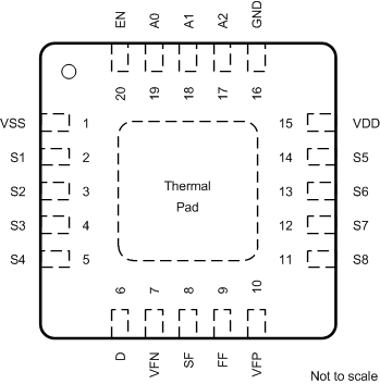
 Figure 6-2 RTJ Package, 20-Pin WQFN
(Top View)
Figure 6-2 RTJ Package, 20-Pin WQFN
(Top View)Table 6-1 Pin Functions: TMUX7348F
| PIN | TYPE(1) | DESCRIPTION | ||
|---|---|---|---|---|
| NAME | TSSOP | WQFN | ||
| A0 | 1 | 19 | I | Logic control input address 0 (A0). The pin has a 4-MΩ internal pull-down resistor. This pin can also be used together with the specific fault pin (SF) to indicate which input is under fault. For more details, see Section 9.4.3. |
| A1 | 20 | 18 | I | Logic control input address 1 (A1). The pin has a 4-MΩ internal pull-down resistor. This pin can also be used together with the specific fault pin (SF) to indicate which input is under fault. For more details, see Section 9.4.3. |
| A2 | 19 | 17 | I | Logic control input address 2 (A2). The pin has a 4-MΩ internal pull-down resistor. This pin can also be used together with the specific fault pin (SF) to indicate which input is under fault. For more details, see Section 9.4.3. |
| D | 8 | 6 | I/O | Drain pin. Can be an input or output. The drain pin is not overvoltage protected and shall remain within the recommended operating range. |
| EN | 2 | 20 | I | Active high logic enable (EN) pin. The pin has a 4-MΩ internal pull-down resistor. The device is disabled and all switches become high impedance when the pin is low. When the pin is high, the Ax logic inputs determine individual switch states. For more details, see Section 9.4.3. |
| FF | 11 | 9 | O | General fault flag. This pin is an open drain output and is asserted low when overvoltage condition is detected on any of the source (Sx) input pins. Connect this pin to an external supply (1.8 V to 5.5 V) through a 1-kΩ pull-up resistor. |
| GND | 18 | 16 | P | Ground (0 V) reference. |
| S1 | 4 | 2 | I/O | Overvoltage protected source pin 1. Can be an input or output. |
| S2 | 5 | 3 | I/O | Overvoltage protected source pin 2. Can be an input or output. |
| S3 | 6 | 4 | I/O | Overvoltage protected source pin 3. Can be an input or output. |
| S4 | 7 | 5 | I/O | Overvoltage protected source pin 4. Can be an input or output. |
| S5 | 16 | 14 | I/O | Overvoltage protected source pin 5. Can be an input or output. |
| S6 | 15 | 13 | I/O | Overvoltage protected source pin 6. Can be an input or output. |
| S7 | 14 | 12 | I/O | Overvoltage protected source pin 7. Can be an input or output. |
| S8 | 13 | 11 | I/O | Overvoltage protected source pin 8. Can be an input or output. |
| SF | 10 | 8 | O | Specific fault flag. Table 9-1 shows how this pin is an open drain output and is asserted low when overvoltage condition is detected on a specific pin, depending on the state of A0, A1, and A2. Connect this pin to an external supply (1.8 V to 5.5 V) through a 1-kΩ pull-up resistor. |
| VDD | 17 | 15 | P | Positive power supply. This pin is the most positive power-supply potential. For reliable operation, connect a decoupling capacitor ranging from 0.1 µF to 10 µF between VDD and GND. |
| VFN | 9 | 7 | P | Negative fault voltage supply that determines the overvoltage protection triggering threshold on the negative side. Connect to VSS if the triggering threshold will be the same as the device's negative supply. For reliable operation, connect a decoupling capacitor ranging from 0.1 µF to 10 µF between VFN and GND. |
| VFP | 12 | 10 | P | Positive fault voltage supply that determines the overvoltage protection triggering threshold on the positive side. Connect to VDD if the triggering threshold will be the same as the device's positive supply. For reliable operation, connect a decoupling capacitor ranging from 0.1 µF to 10 µF between VFP and GND. |
| VSS | 3 | 1 | P | Negative power supply. This pin is the most negative power-supply potential. In single-supply applications, this pin can be connected to ground. For reliable operation, connect a decoupling capacitor ranging from 0.1 µF to 10 µF between VSS and GND. |
| Thermal Pad | — | Thermal pad. The thermal pad is not connected internally. It is recommended that the pad be tied to GND or VSS for best performance. | ||
(1) I = input, O = output, I/O = input and output, P = power
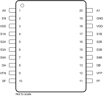
 Figure 6-3 PW Package, 20-Pin TSSOP
(Top View)
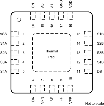
 Figure 6-4 RTJ Package, 20-Pin WQFN
(Top View)
Figure 6-4 RTJ Package, 20-Pin WQFN
(Top View)Table 6-2 Pin Functions: TMUX7349F
| PIN | TYPE(1) | DESCRIPTION | ||
|---|---|---|---|---|
| NAME | TSSOP | WQFN | ||
| A0 | 1 | 19 | I | Logic control input address 0 (A0). The pin has a 4-MΩ internal pull-down resistor. This pin can also be used together with the specific fault pin (SF) to indicate which input is under fault. For more details, see Section 9.4.3. |
| A1 | 20 | 18 | I | Logic control input address 1 (A1). The pin has a 4-MΩ internal pull-down resistor. This pin can also be used together with the specific fault pin (SF) to indicate which input is under fault. For more details, see Section 9.4.3. |
| DA | 8 | 6 | I/O | Drain terminal A. Can be an input or output. The drain pin is not overvoltage protected and shall remain within the recommended operating range. |
| DB | 13 | 11 | I/O | Drain terminal B. Can be an input or output. The drain pin is not overvoltage protected and shall remain within the recommended operating range. |
| EN | 2 | 20 | I | Active high logic enable (EN) pin. The pin has a 4-MΩ internal pull-down resistor. The device is disabled and all switches become high impedance when the pin is low. When the pin is high, the Ax logic inputs determine individual switch states. This pin can also be used together with the specific fault pin (SF) to indicate which input is under fault. For more details, see Section 9.4.3. |
| FF | 11 | 9 | O | General fault flag. This pin is an open drain output and is asserted low when overvoltage condition is detected on any of the source (Sx) input pins. Connect this pin to an external supply (1.8 V to 5.5 V) through a 1-kΩ pull-up resistor. |
| GND | 19 | 17 | P | Ground (0 V) reference |
| S1A | 4 | 2 | I/O | Overvoltage protected source pin 1A. Can be an input or output. |
| S1B | 17 | 15 | I/O | Overvoltage protected source pin 1B. Can be an input or output. |
| S2A | 5 | 3 | I/O | Overvoltage protected source pin 2A. Can be an input or output. |
| S2B | 16 | 14 | I/O | Overvoltage protected source pin 2B. Can be an input or output. |
| S3A | 6 | 4 | I/O | Overvoltage protected source pin 3A. Can be an input or output. |
| S3B | 15 | 13 | I/O | Overvoltage protected source pin 3B. Can be an input or output. |
| S4A | 7 | 5 | I/O | Overvoltage protected source pin 4A. Can be an input or output. |
| S4B | 14 | 12 | I/O | Overvoltage protected source pin 4B. Can be an input or output. |
| SF | 10 | 8 | O | Specific fault flag. Table 9-2 provides how this pin is an open drain output and is asserted low when overvoltage condition is detected on a specific pin, depending on the state of A0, A1, and EN. Connect this pin to an external supply (1.8 V to 5.5 V) through a 1-kΩ pull-up resistor. |
| VDD | 18 | 16 | P | Positive power supply. This pin is the most positive power-supply potential. For reliable operation, connect a decoupling capacitor ranging from 0.1 µF to 10 µF between VDD and GND. |
| VFN | 9 | 7 | P | Negative fault voltage supply that determines the overvoltage protection triggering threshold on the negative side. Connect to VSS if the triggering threshold will be the same as the device's negative supply. For reliable operation, connect a decoupling capacitor ranging from 0.1 µF to 10 µF between VFN and GND. |
| VFP | 12 | 10 | P | Positive fault voltage supply that determines the overvoltage protection triggering threshold on the positive side. Connect to VDD if the triggering threshold will be the same as the device's positive supply. For reliable operation, connect a decoupling capacitor ranging from 0.1 µF to 10 µF between VFP and GND. |
| VSS | 3 | 1 | P | Negative power supply. This pin is the most negative power-supply potential. In single-supply applications, this pin can be connected to ground. For reliable operation, connect a decoupling capacitor ranging from 0.1 µF to 10 µF between VSS and GND. |
| Thermal Pad | — | Thermal pad. The thermal pad is not connected internally. It is recommended to tie the pad to GND or VSS for best performance. | ||
(1) I = input, O = output, I/O = input and output, P = power