SCDS404B March 2021 – November 2022 TMUX7411F , TMUX7412F , TMUX7413F
PRODMIX
- 1 Features
- 2 Applications
- 3 Description
- 4 Revision History
- 5 Device Comparison Table
- 6 Pin Configuration and Functions
-
7 Specifications
- 7.1 Absolute Maximum Ratings
- 7.2 ESD Ratings
- 7.3 Thermal Information
- 7.4 Recommended Operating Conditions
- 7.5 Electrical Characteristics: Global
- 7.6 ±15 V Dual Supply: Electrical Characteristics
- 7.7 ±20 V Dual Supply: Electrical Characteristics
- 7.8 12 V Single Supply: Electrical Characteristics
- 7.9 36 V Single Supply: Electrical Characteristics
- 7.10 Typical Characteristics
-
8 Parameter Measurement Information
- 8.1 On-Resistance
- 8.2 Turn-On and Turn-Off Time
- 8.3 Off-Leakage Current
- 8.4 On-Leakage Current
- 8.5 Input and Output Leakage Current Under Overvoltage Fault
- 8.6 Fault Response Time
- 8.7 Fault Recovery Time
- 8.8 Fault Flag Response Time
- 8.9 Fault Flag Recovery Time
- 8.10 Charge Injection
- 8.11 Off Isolation
- 8.12 Inter-Channel Crosstalk
- 8.13 Bandwidth
- 8.14 THD + Noise
- 9 Detailed Description
- 10Application and Implementation
- 11Power Supply Recommendations
- 12Layout
- 13Device and Documentation Support
- 14Mechanical, Packaging, and Orderable Information
Package Options
Mechanical Data (Package|Pins)
- RRP|16
Thermal pad, mechanical data (Package|Pins)
Orderable Information
10.2.3 Application Curves
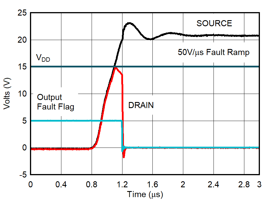
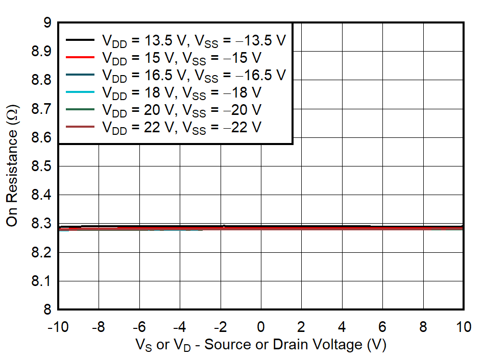
The previous example shows how the fault protection of the TMUX741xF is utilized to protect downstream components from damage due to incorrect wiring connections from the power module. Figure 10-2 shows an example of positive overvoltage fault response with a fast fault ramp rate of 50 V/µs. Figure 10-3 shows the extremely flat on-resistance across source voltage while operating within a common signal range of ±10 V. These features make the TMUX741xF an ideal solution for factory automation applications that may face various fault conditions but also require excellent linearity and low distortion.
 Figure 10-2 Positive Overvoltage Response
 Figure 10-3 RON Flatness in Non-Fault Region