SCDS435B september 2021 – august 2023 TMUX8108 , TMUX8109
PRODUCTION DATA
- 1
- 1 Features
- 2 Applications
- 3 Description
- 4 Revision History
- 5 Device Comparison Table
- 6 Pin Configuration and Functions
-
7 Specifications
- 7.1 Absolute Maximum Ratings: TMUX810x Devices
- 7.2 ESD Ratings
- 7.3 Recommended Operating Conditions: TMUX810x Devices
- 7.4 Thermal Information
- 7.5 Electrical Characteristics (Global): TMUX810x Devices
- 7.6 Electrical Characteristics (±15-V Dual Supply)
- 7.7 Electrical Characteristics (±36-V Dual Supply)
- 7.8 Electrical Characteristics (±50-V Dual Supply)
- 7.9 Electrical Characteristics (72-V Single Supply)
- 7.10 Electrical Characteristics (100-V Single Supply)
- 7.11 Switching Characteristics: TMUX810x Devices
- 7.12 Typical Characteristics
- 8 Parameter Measurement Information
- 9 Detailed Description
- 10Application and Implementation
- 11Device and Documentation Support
- 12Mechanical, Packaging, and Orderable Information
Package Options
Refer to the PDF data sheet for device specific package drawings
Mechanical Data (Package|Pins)
- PW|16
- RUM|16
Thermal pad, mechanical data (Package|Pins)
- RUM|16
Orderable Information
8.1 On-Resistance
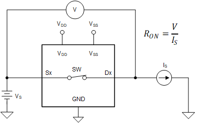
The on-resistance of the TMUX8108 and TMUX8109 is the ohmic resistance across the source (Sx) and drain (Dx) pins of the device. The on-resistance varies with input voltage and supply voltage. Figure 8-1 shows how the symbol RON is used to denote on-resistance. The measurement setup used to measure RON is also shown in the following figure. ΔRON represents the difference between the RON of any two channels, while RON_FLAT denotes the flatness that is defined as the difference between the maximum and minimum value of on-resistance measured over the specified analog signal range.
 Figure 8-1 On-Resistance Measurement Setup