SLASF52A August 2022 – November 2022 TMUXHS221
PRODUCTION DATA
- 1 Features
- 2 Applications
- 3 Description
- 4 Revision History
- 5 Pin Configuration and Functions
-
6 Specifications
- 6.1 Absolute Maximum Ratings
- 6.2 ESD Ratings
- 6.3 Recommended Operating Conditions
- 6.4 Thermal Information
- 6.5 Electrical Characteristics
- 6.6 High-Speed Performance Parameters
- 6.7 Switching Characteristics
- 6.8 Typical Characteristics – S-Parameters
- 6.9 Typical Characteristics – Eye Diagrams
- 16
- 6.10 Typical Characteristics – RON
- 7 Detailed Description
- 8 Application and Implementation
- 9 Power Supply Recommendations
- 10Layout
- 11Device and Documentation Support
- 12Mechanical, Packaging, and Orderable Information
Package Options
Mechanical Data (Package|Pins)
- NKG|10
Thermal pad, mechanical data (Package|Pins)
Orderable Information
8.2.1.3 Application Curves
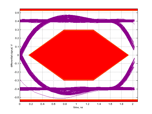
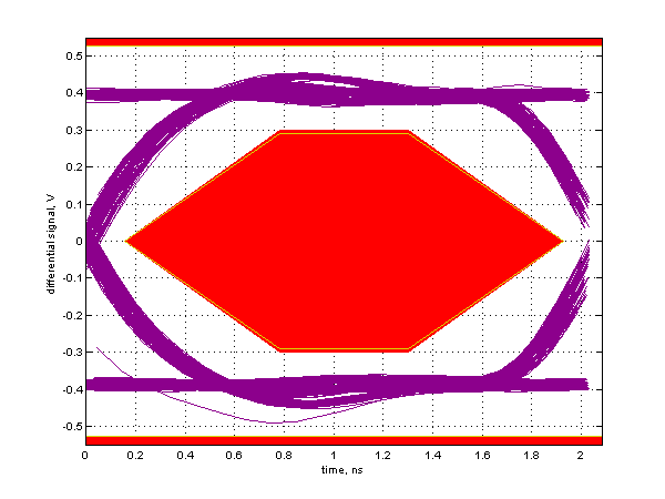
Figure 8-2 and Figure 8-3 show eye diagrams for USB 2.0 signals through calibration traces (without device) and TMUXHS221 channel. A combination of very low channel ON resistance, high bandwidth, very low reflection (retun loss), and low added jitter from the device allows 480 MBps USB 2.0 HS signals to stay almost unattenuated. Many system platforms struggle to pass USB 2.0 compliance due to high loss. TMUXHS221 allows insertion of an analog mux device in the signal path without creating any additional signal integrity challenge.
 Figure 8-2 USB 2.0 HS
Compliance Eye in TI Evaluation Board – Through Calibration Traces
  Figure 8-3 USB 2.0 HS Compliance Eye in TI Evaluation Board – Through TMUXHS221
Channel