SLOS942 April 2018 TPA3126D2
PRODUCTION DATA.
- 1 Features
- 2 Applications
- 3 Description
- 4 Revision History
- 5 Device Comparison Table
- 6 Pin Configuration and Functions
- 7 Specifications
-
8 Detailed Description
- 8.1 Overview
- 8.2 Functional Block Diagram
- 8.3
Feature Description
- 8.3.1 Gain Setting and Master and Slave
- 8.3.2 Input Impedance
- 8.3.3 Startup and Shutdown Operation
- 8.3.4 PLIMIT Operation
- 8.3.5 GVDD Supply
- 8.3.6 BSPx and BSNx Capacitors
- 8.3.7 Differential Inputs
- 8.3.8 Device Protection System
- 8.3.9 DC Detect Protection
- 8.3.10 Short-Circuit Protection and Automatic Recovery Feature
- 8.3.11 Thermal Protection
- 8.3.12 Device Modulation Scheme
- 8.3.13 Efficiency: LC Filter Required with the Traditional Class-D Modulation Scheme
- 8.3.14 Ferrite Bead Filter Considerations
- 8.3.15 When to Use an Output Filter for EMI Suppression
- 8.3.16 AM Avoidance EMI Reduction
- 8.4 Device Functional Modes
- 9 Application and Implementation
- 10Power Supply Recommendations
- 11Layout
- 12Device and Documentation Support
- 13Mechanical, Packaging, and Orderable Information
Package Options
Mechanical Data (Package|Pins)
- DAD|32
Thermal pad, mechanical data (Package|Pins)
- DAD|32
Orderable Information
8.3.1 Gain Setting and Master and Slave
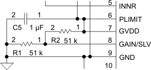
The gain of the TPA3126D2 is set by the voltage divider connected to the GAIN/SLV control pin. Master or Slave mode is also controlled by the same pin. An internal ADC is used to detect the 8 input states. The first four states set the GAIN in Master mode with gains of 20, 26, 32, and 36 dB respectively, while the next four states set the GAIN in Slave mode with gains of 20, 26, 32, and 36 dB respectively. The gain setting is latched during power-up and cannot be changed while the device is powered on. Table 1 lists the recommended resistor values for different state settings.
Table 1. Gain and Master/Slave
| MASTER / SLAVE MODE | GAIN | R1 (to GND)(1) | R2 (to GVDD)(1) | INPUT IMPEDANCE |
|---|---|---|---|---|
| Master | 20 dB | 5.6 kΩ | OPEN | 60 kΩ |
| Master | 26 dB | 20 kΩ | 100 kΩ | 30 kΩ |
| Master | 32 dB | 39 kΩ | 100 kΩ | 15 kΩ |
| Master | 36 dB | 47 kΩ | 75 kΩ | 9 kΩ |
| Slave | 20 dB | 51 kΩ | 51 kΩ | 60 kΩ |
| Slave | 26 dB | 75 kΩ | 47 kΩ | 30 kΩ |
| Slave | 32 dB | 100 kΩ | 39 kΩ | 15 kΩ |
| Slave | 36 dB | 100 kΩ | 16 kΩ | 9 kΩ |
 Figure 25. Gain, Master/Slave
In Master mode, the SYNC terminal is an output, while in Slave mode, the SYNC terminal is an input for a clock. TTL logic levels with compliance to GVDD.