SLOS941C May 2016 – January 2018 TPA3128D2 , TPA3129D2
PRODUCTION DATA.
- 1 Features
- 2 Applications
- 3 Description
- 4 Revision History
- 5 Pin Configuration and Functions
- 6 Specifications
-
7 Detailed Description
- 7.1 Overview
- 7.2 Functional Block Diagram
- 7.3
Feature Description
- 7.3.1 Gain Setting and Master and Slave
- 7.3.2 Input Impedance
- 7.3.3 Startup and Shutdown Operation
- 7.3.4 PLIMIT Operation
- 7.3.5 GVDD Supply
- 7.3.6 BSPx AND BSNx Capacitors
- 7.3.7 Differential Inputs
- 7.3.8 Device Protection System
- 7.3.9 DC Detect Protection
- 7.3.10 Short-Circuit Protection and Automatic Recovery Feature
- 7.3.11 Thermal Protection
- 7.3.12 Device Modulation Scheme
- 7.3.13 Efficiency: LC Filter Required with the Traditional Class-D Modulation Scheme
- 7.3.14 Ferrite Bead Filter Considerations
- 7.3.15 When to Use an Output Filter for EMI Suppression
- 7.3.16 AM Avoidance EMI Reduction
- 7.4 Device Functional Modes
- 8 Applications and Implementation
- 9 Power Supply Recommendations
- 10Layout
- 11Device and Documentation Support
- 12Mechanical, Packaging, and Orderable Information
Package Options
Mechanical Data (Package|Pins)
- DAP|32
Thermal pad, mechanical data (Package|Pins)
- DAP|32
Orderable Information
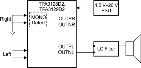
7.4.2 Mono Mode (Single Channel Mode)
The and TPA3129D2 can be connected in MONO mode to cut the idle power-loss nearly by half. This is done by:
- Connect INPR and INNR directly to Ground (without capacitors) this sets the device in Mono mode during power up.
- Connect OUTPL and OUTNL to speaker just like normal BTL mode.
- Analog input signal is applied to INPL and INNL.
 Figure 35. MONO Mode