SLASEN3B January 2018 – August 2018 TPA3220
PRODUCTION DATA.
- 1 Features
- 2 Applications
- 3 Description
- 4 Revision History
- 5 Device Comparison Table
- 6 Pin Configuration and Functions
-
7 Specifications
- 7.1 Absolute Maximum Ratings
- 7.2 ESD Ratings
- 7.3 Recommended Operating Conditions
- 7.4 Thermal Information
- 7.5 Electrical Characteristics
- 7.6 Audio Characteristics (BTL)
- 7.7 Audio Characteristics (PBTL)
- 7.8 Typical Characteristics, BTL Configuration, AD-mode
- 7.9 Typical Characteristics, PBTL Configuration, AD-mode
- 8 Parameter Measurement Information
-
9 Detailed Description
- 9.1 Overview
- 9.2 Functional Block Diagrams
- 9.3 Feature Description
- 9.4
Device Functional Modes
- 9.4.1 Powering Up
- 9.4.2 Powering Down
- 9.4.3 Device Reset
- 9.4.4 Device Soft Mute
- 9.4.5
Device Protection System
- 9.4.5.1 Overload and Short Circuit Current Protection
- 9.4.5.2 Signal Clipping and Pulse Injector
- 9.4.5.3 DC Speaker Protection
- 9.4.5.4 Pin-to-Pin Short Circuit Protection (PPSC)
- 9.4.5.5 Overtemperature Protection OTW and OTE
- 9.4.5.6 Undervoltage Protection (UVP) and Power-on Reset (POR)
- 9.4.5.7 Fault Handling
- 10Application and Implementation
- 11Power Supply Recommendations
- 12Layout
- 13Device and Documentation Support
- 14Mechanical, Packaging, and Orderable Information
Package Options
Refer to the PDF data sheet for device specific package drawings
Mechanical Data (Package|Pins)
- DDW|44
Thermal pad, mechanical data (Package|Pins)
Orderable Information
9.3.2 Gain Setting And Master / Slave Operation
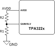
The gain of TPA3220 is set by the voltage divider connected to the GAIN/SLV control pin. Master or Slave mode is also controlled by the same pin. An internal ADC is used to detect the 8 input states. The first four stages sets the GAIN in Master mode in gains of 18, 24, 30, 34 dB respectively, while the next four stages sets the GAIN in Slave mode in gains of 18, 24, 30, 34 dB respectively. The gain setting is latched when RESET goes high and cannot be changed while RESET is high. Table 2 shows the recommended resistor values, the state and gain:
Table 2. Gain and Master / Slave
| Master / Slave Mode | Gain | R1 (to GND) | R2 (to AVDD) | Differential Input Signal Level
(each input pin) |
Single Ended Input Signal Level |
|---|---|---|---|---|---|
| Master | 18 dB | 5.6 kΩ | OPEN | 2 VRMS | 2 VRMS |
| Master | 24 dB | 20 kΩ | 100 kΩ | 1 VRMS | 2 VRMS |
| Master | 30 dB | 39 kΩ | 100 kΩ | 0.5 VRMS | 1 VRMS |
| Master | 34 dB | 47 kΩ | 75 kΩ | 0.32 VRMS | 0.63 VRMS |
| Slave | 18 dB | 51 kΩ | 51 kΩ | 2 VRMS | 2 VRMS |
| Slave | 24 dB | 75 kΩ | 47 kΩ | 1 VRMS | 2 VRMS |
| Slave | 30 dB | 100 kΩ | 39 kΩ | 0.5 VRMS | 1 VRMS |
| Slave | 34 dB | 100 kΩ | 16 kΩ | 0.32 VRMS | 0.63 VRMS |
 Figure 32. Gain and Master / Slave Setup
 For easy multi-channel system design TPA3220 has a Master / Slave feature that allows automatic synchronization of multiple slave devices operated at the PWM switching frequency of a master device. This benefits system noise performance by eliminating spurious crosstalk sum and difference tones due to unsynchronized channel-to-channel switching frequencies. Furthermore the Master / Slave scheme is designed to interleave switching of the individual channels in a multi-channel system such that the power supply current ripple frequency is moved to a higher frequency which reduces the RMS ripple current in the power supply bulk capacitors.
The Master / Slave scheme and the interleaving of the output stage switching is automatically configured by connecting the OSCx pins between a master and multiple slave devices. Connect the OSCx pins in either positive or negative polarity to configure either a Slave1 or Slave2 device. Connect the OSCM of the Master device to the OSCM of a slave device to configure for Slave1 or OSCP to configure for Slave2. Then connect the remaining OSCx pins between the master and slave devices. The Master, Slave1 and Slave2 PWM switching will be 30 degrees out of phase with each other. All switching channels are automatically synchronized by releasing RESET on all devices at the same time.
 Figure 33. Gain and Master PCB Implementation
 Placement on the PCB and connection of multiple TPA3220 devices in a multi channel system is illustrated in Figure 33. Slave devices should be placed on either side of the master device, with a Slave1 device on one side of the Master device, and a Slave2 device on the other. In systems with more than 3 TPA3220 devices, the master should be in the middle, and every second slave devices should be a Slave1 or Slave 2 as illustrated in Figure 33. A 47kΩ pull up resistor to AVDD should be connected to the master device OSCM output and a 47kΩ pull down resistor to GND should be connected to the master OSCP CLK outputs.