SLASEE9B September 2017 – December 2017 TPA3221
PRODUCTION DATA.
- 1 Features
- 2 Applications
- 3 Description
- 4 Revision History
- 5 Device Comparison Table
- 6 Pin Configuration and Functions
-
7 Specifications
- 7.1 Absolute Maximum Ratings
- 7.2 ESD Ratings
- 7.3 Recommended Operating Conditions
- 7.4 Thermal Information
- 7.5 Electrical Characteristics
- 7.6 Audio Characteristics (BTL)
- 7.7 Audio Characteristics (PBTL)
- 7.8 Typical Characteristics, BTL Configuration, AD-mode
- 7.9 Typical Characteristics, PBTL Configuration, AD-mode
- 8 Parameter Measurement Information
-
9 Detailed Description
- 9.1 Overview
- 9.2 Functional Block Diagrams
- 9.3 Feature Description
- 9.4
Device Functional Modes
- 9.4.1 Powering Up
- 9.4.2 Powering Down
- 9.4.3 Device Reset
- 9.4.4 Device Soft Mute
- 9.4.5
Device Protection System
- 9.4.5.1 Overload and Short Circuit Current Protection
- 9.4.5.2 Signal Clipping and Pulse Injector
- 9.4.5.3 DC Speaker Protection
- 9.4.5.4 Pin-to-Pin Short Circuit Protection (PPSC)
- 9.4.5.5 Overtemperature Protection OTW and OTE
- 9.4.5.6 Undervoltage Protection (UVP), Overvoltage Protection (OVP) and Power-on Reset (POR)
- 9.4.5.7 Fault Handling
- 10Application and Implementation
- 11Power Supply Recommendations
- 12Layout
- 13Device and Documentation Support
- 14Mechanical, Packaging, and Orderable Information
Package Options
Mechanical Data (Package|Pins)
- DDV|44
Thermal pad, mechanical data (Package|Pins)
- DDV|44
Orderable Information
10 Application and Implementation
NOTE
Information in the following applications sections is not part of the TI component specification, and TI does not warrant its accuracy or completeness. TI’s customers are responsible for determining suitability of components for their purposes. Customers should validate and test their design implementation to confirm system functionality.
10.1 Application Information
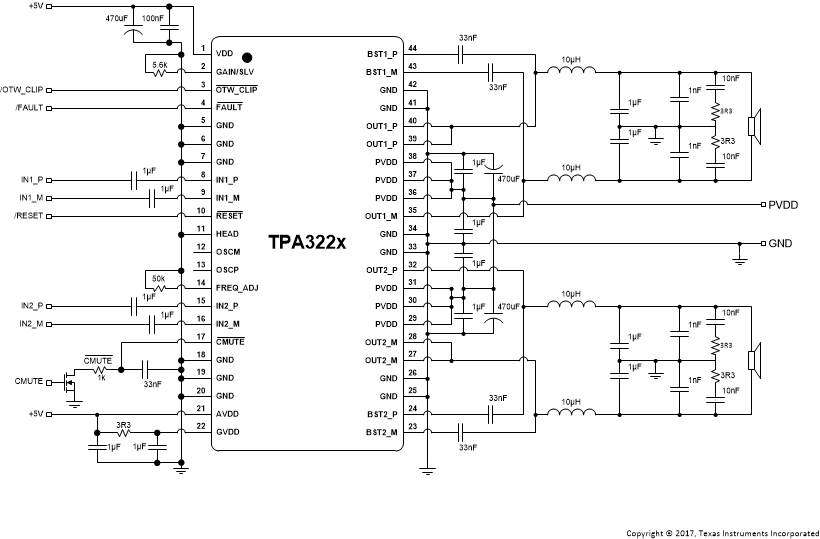
TPA3221 can be configured either in stereo BTL, mono BTL or mono PBTL mode depending on output power conditions and system design.
10.2 Typical Applications
10.2.1 Stereo BTL Application
10.2.1.1 Design Requirements
For this design example, use the parameters in Table 7.
Table 7. Design Requirements, BTL Application
| DESIGN PARAMETER | EXAMPLE |
|---|---|
| ExternalLow Power Supply | 5 V |
| High Power Supply | 7 - 30 V |
| Analog Inputs | IN1_M = ±2.8V (peak, max) |
| IN1_P = ±2.8V (peak, max) | |
| IN2_M = ±2.8V (peak, max) | |
| IN2_P = ±2.8V (peak, max) | |
| Output Filters | Inductor-Capacitor Low Pass FIlter (10 µH + 1 µF) |
| Speaker Impedance | 3 - 8 Ω |
10.2.1.2 Detailed Design Procedures
A rising-edge transition on RESET input allows the device to execute the startup sequence and starts switching.
A toggling OTW_CLIP signal is indicating that the output is approaching clipping. The signal can be used either to decrease audio volume or to control an intelligent power supply nominally operating at a low rail adjusting to a higher supply rail.
The device inverts the audio signal from input to output.
The AVDD pin is not recommended to be used as a voltage source for external circuitry when internal LDO is enabled (VDD ≥ 7 V).
10.2.1.2.1 Decoupling Capacitor Recommendations
In order to design an amplifier that has robust performance, passes regulatory requirements, and exhibits good audio performance, good quality decoupling capacitors should be used. In practice, X7R should be used in this application.
The voltage of the decoupling capacitors should be selected in accordance with good design practices. Temperature, ripple current, and voltage overshoot must be considered. This fact is particularly true in the selection of the 1μF that is placed on the power supply to each full-bridge. It must withstand the voltage overshoot of the PWM switching, the heat generated by the amplifier during high power output, and the ripple current created by high power output. A minimum voltage rating of 50 V is required for use with a 30 V power supply.
10.2.1.2.2 PVDD Capacitor Recommendation
The large capacitors used in conjunction with each full-bridge, are referred to as the PVDD Capacitors. These capacitors should be selected for proper voltage margin and adequate capacitance to support the power requirements. In practice, with a well designed system power supply, 470 μF, 50 V supports most applications. The PVDD capacitors should be low ESR type because they are used in a circuit associated with high-speed switching.
10.2.1.2.3 BST capacitors
To ensure large enough bootstrap energy storage for the high side gate drive to work correctly with all audio source signals, 33 nF / 50V X7R BST capacitors are recommended.
10.2.1.2.4 PCB Material Recommendation
FR-4 Glass Epoxy material with 2 oz. (70 μm) copper is recommended for use with the TPA3221. The use of this material can provide for higher power output, improved thermal performance, and better EMI margin (due to lower PCB trace inductance.
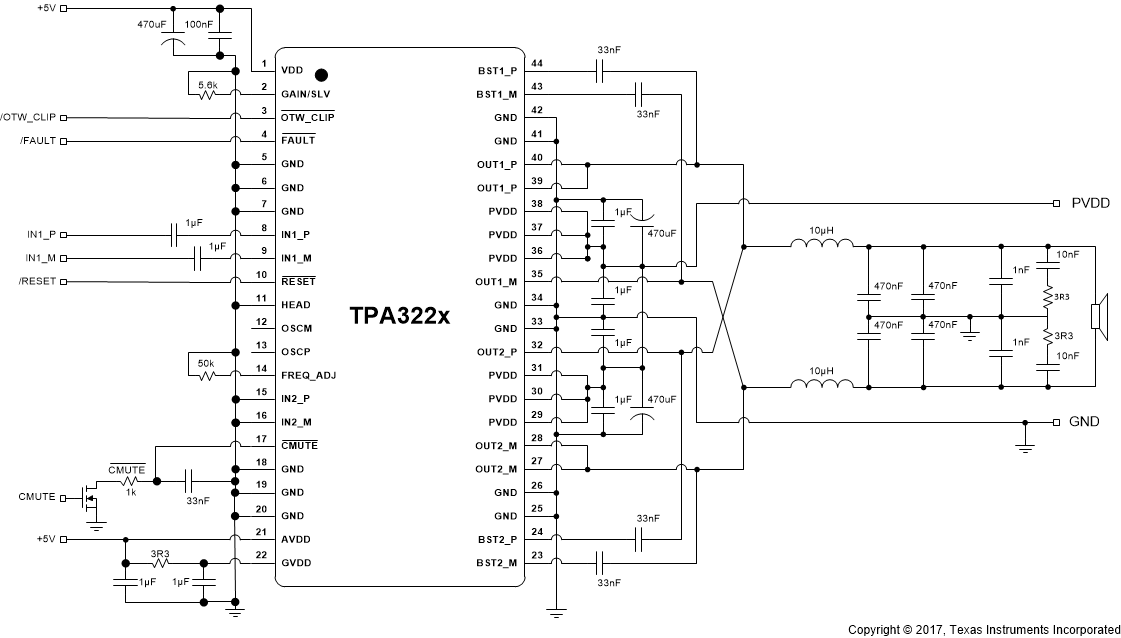
10.2.2 Typical Application, Differential (2N), AD-Mode PBTL (Outputs Paralleled before LC filter)
TPA3221 can be configured in mono PBTL mode by paralleling the outputs before the LC filter or after the LC filter (see Typical Application, Differential (2N), AD-Mode PBTL (Outputs Paralleled after LC filter)). Paralleled outputs before the LC filter is recommended for better performance and limiting the number of output LC filter inductors,
10.2.2.1 Design Requirements
Refer to Stereo BTL Application for the Design Requirements.
Table 8. Design Requirements, PBTL Application
| DESIGN PARAMETER | EXAMPLE |
|---|---|
| Low Power Supply | 5 V |
| High Power Supply | 7 - 30 V |
| Analog Inputs | IN1_M = ±2.8 V (peak, max) |
| IN1_P = ±2.8 V (peak, max) | |
| IN2_M = Grounded | |
| IN2_P = Grounded | |
| Output Filters | Inductor-Capacitor Low Pass FIlter (10 µH + 1 µF) |
| Speaker Impedance | 2 - 4 Ω |
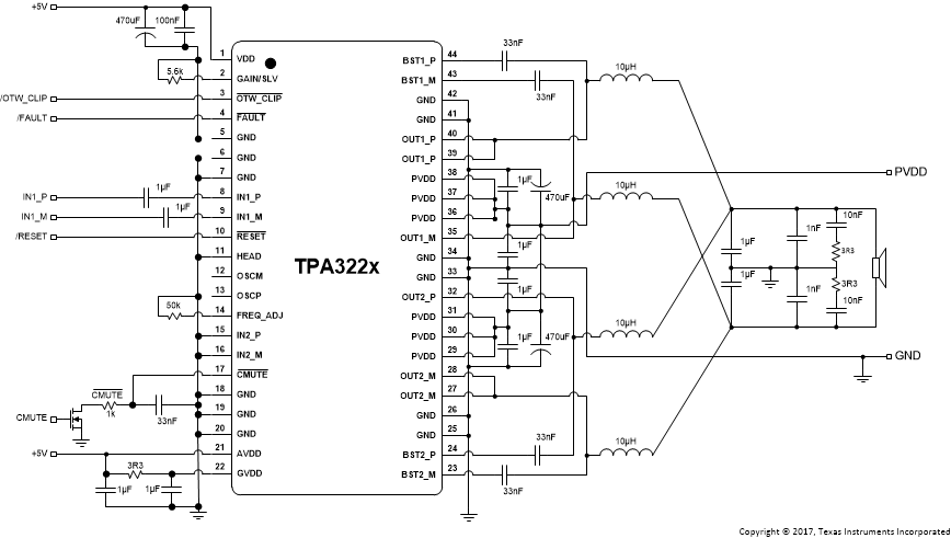
10.2.3 Typical Application, Differential (2N), AD-Mode PBTL (Outputs Paralleled after LC filter)
TPA3221 can be configured in mono PBTL mode by paralleling the outputs before the LC filter (see Typical Application, Differential (2N), AD-Mode PBTL (Outputs Paralleled before LC filter)) or after the LC filter. Paralleled outputs after the LC filter may be preferred if: a single board design must support both PBTL and BTL, or in the case multiple, smaller paralleled inductors are preferred due to size or cost. Paralleling after the LC filter requires four inductors, one for each OUT_x. This section shows an example of paralleled outputs after the LC filter.
10.2.3.1 Design Requirements
Refer to Stereo BTL Application for the Design Requirements.
Table 9. Design Requirements, PBTL Application
| DESIGN PARAMETER | EXAMPLE |
|---|---|
| Low Power Supply | 5 V |
| High Power Supply | 7 - 30 V |
| Analog Inputs | IN1_M = ±2.8 V (peak, max) |
| IN1_P = ±2.8 V (peak, max) | |
| IN2_M = Grounded | |
| IN2_P = Grounded | |
| Output Filters | Inductor-Capacitor Low Pass FIlter (10 µH + 1 µF) |
| Speaker Impedance | 2 - 4 Ω |


