SLASEM8A January 2019 – March 2019 TPA3255-Q1
PRODUCTION DATA.
- 1 Features
- 2 Applications
- 3 Description
- 4 Revision History
- 5 Pin Configuration and Functions
-
6 Specifications
- 6.1 Absolute Maximum Ratings
- 6.2 ESD Ratings
- 6.3 Recommended Operating Conditions
- 6.4 Thermal Information
- 6.5 Electrical Characteristics
- 6.6 Audio Characteristics (BTL)
- 6.7 Audio Characteristics (SE)
- 6.8 Audio Characteristics (PBTL)
- 6.9 Typical Characteristics, BTL Configuration
- 6.10 Typical Characteristics, SE Configuration
- 6.11 Typical Characteristics, PBTL Configuration
- 7 Parameter Measurement Information
-
8 Detailed Description
- 8.1 Overview
- 8.2 Functional Block Diagrams
- 8.3 Feature Description
- 8.4
Device Functional Modes
- 8.4.1
Device Protection System
- 8.4.1.1 Overload and Short Circuit Current Protection
- 8.4.1.2 Signal Clipping and Pulse Injector
- 8.4.1.3 DC Speaker Protection
- 8.4.1.4 Pin-to-Pin Short Circuit Protection (PPSC)
- 8.4.1.5 Overtemperature Protection OTW and OTE
- 8.4.1.6 Undervoltage Protection (UVP) and Power-on Reset (POR)
- 8.4.1.7 Fault Handling
- 8.4.1.8 Device Reset
- 8.4.1
Device Protection System
- 9 Application and Implementation
- 10Power Supply Recommendations
- 11Layout
- 12Device and Documentation Support
- 13Mechanical, Packaging, and Orderable Information
Package Options
Mechanical Data (Package|Pins)
- DDV|44
Thermal pad, mechanical data (Package|Pins)
- DDV|44
Orderable Information
8.4.1.1 Overload and Short Circuit Current Protection
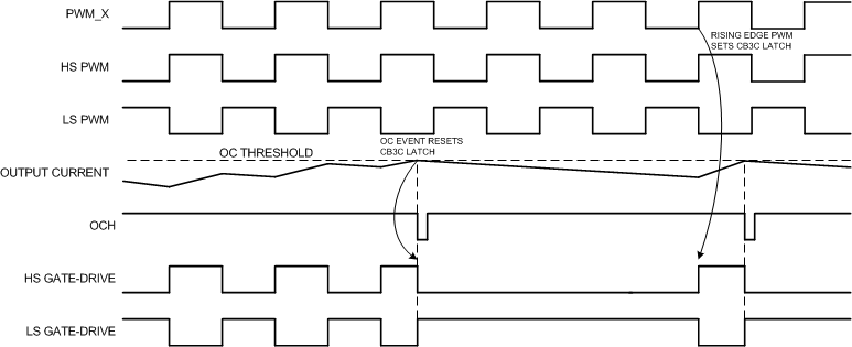
TPA3255-Q1 has fast reacting current sensors with a programmable trip threshold (OC threshold) on all high-side and low-side FETs. To prevent output current from increasing beyond the programmed threshold, TPA3255-Q1 has the option of either limiting the output current for each switching cycle (Cycle By Cycle Current Control, CB3C) or to perform an immediate shutdown of the output in case of excess output current (Latching Shutdown). CB3C prevents premature shutdown due to high output current transients caused by high level music transients and a drop of real speaker’s load impedance, and allows the output current to be limited to a maximum programmed level. If the maximum output current persists, i.e. the power stage being overloaded with too low load impedance, the device will shut down the affected output channel and the affected output is put in a high-impedance (Hi- Z) state until a RESET cycle is initiated. CB3C works individually for each half bridge output. If an over current event is triggered, CB3C performs a state flip of the half bridge output that is cleared upon beginning of next PWM frame.
 Figure 26. CB3C Timing Example
 During CB3C an over load counter increments for each over current event and decrease for each non-over current PWM cycle. This allows full amplitude transients into a low speaker impedance without a shutdown protection action. In the event of a short circuit condition, the over current protection limits the output current by the CB3C operation and eventually shut down the affected output if the overload counter reaches its maximum value. If a latched OC operation is required such that the device shuts down the affected output immediately upon first detected over current event, this protection mode should be selected. The over current threshold and mode (CB3C or Latched OC) is programmed by the OC_ADJ resistor value. The OC_ADJ resistor needs to be within its intentional value range for either CB3C operation or Latched OC operation.
 Figure 27. OC Threshold versus OC_ADJ Resistor Value Example
 OC_ADJ values outside specified value range for either CB3C or latched OC operation will result in minimum OC threshold.
Table 4. Device Protection
| OC_ADJ Resistor Value | Protection Mode | OC Threshold |
|---|---|---|
| 22kΩ | CB3C | 17.0A |
| 24kΩ | CB3C | 15.7A |
| 27kΩ | CB3C | 14.2A |
| 30kΩ | CB3C | 12.9A |
| 47kΩ | Latched OC | 17.0A |
| 51kΩ | Latched OC | 15.7A |
| 56kΩ | Latched OC | 14.2A |
| 64kΩ | Latched OC | 12.9A |