SLIS113E October   2004  – May 2022 TPIC1021

PRODUCTION DATA  

  1. Features
  2. Applications
  3. Description
  4. Revision History
  5. Description (continued)
  6. Pin Configuration and Functions
  7. Specifications
    1. 7.1 Absolute Maximum Ratings
    2. 7.2 ESD Ratings
    3. 7.3 Recommended Operating Conditions
    4. 7.4 Thermal Information
    5. 7.5 Electrical Characteristics
    6. 7.6 Timing Requirements
    7. 7.7 Typical Characteristics
  8. Detailed Description
    1. 8.1 Overview
    2. 8.2 Functional Block Diagram
    3. 8.3 Feature Description
      1. 8.3.1 LIN Bus Pin
        1. 8.3.1.1 Transmitter Characteristics
        2. 8.3.1.2 Receiver Characteristics
      2. 8.3.2 Transmit Input Pin (TXD)
        1. 8.3.2.1 TXD Dominant State Timeout
      3. 8.3.3 Receive Output Pin (RXD)
        1. 8.3.3.1 RXD Wake-up Request
      4. 8.3.4 Ground (GND)
      5. 8.3.5 Enable Input Pin (EN)
      6. 8.3.6 NWake Input Pin (NWake)
      7. 8.3.7 Inhibit Output Pin (INH)
    4. 8.4 Device Functional Modes
      1. 8.4.1 Operating States
        1. 8.4.1.1 Normal Mode
        2. 8.4.1.2 Low Power Mode
        3. 8.4.1.3 Wake-Up Events
        4. 8.4.1.4 Standby Mode
      2. 8.4.2 Supply Voltage (VSUP)
  9. Application and Implementation
    1. 9.1 Application Information
    2. 9.2 Typical Application
      1. 9.2.1 Design Requirements
      2. 9.2.2 Detailed Design Procedure
      3. 9.2.3 Application Curves
    3. 9.3 Power Supply Recommendations
    4. 9.4 Layout
      1. 9.4.1 Layout Guidelines
      2. 9.4.2 Layout Example
  10. 10Device and Documentation Support
    1. 10.1 Receiving Notification of Documentation Updates
    2. 10.2 Support Resources
    3. 10.3 Trademarks
    4. 10.4 Electrostatic Discharge Caution
    5. 10.5 Glossary
  11. 11Mechanical, Packaging, and Orderable Information

Package Options

Refer to the PDF data sheet for device specific package drawings

Mechanical Data (Package|Pins)
  • D|8
Thermal pad, mechanical data (Package|Pins)
Orderable Information

Application Curves

Figure 9-2 and Figure 9-3 show the propagation delay from the TXD pin to the LIN pin for both the recessive to dominant and dominant to recessive states under lightly loaded conditions.
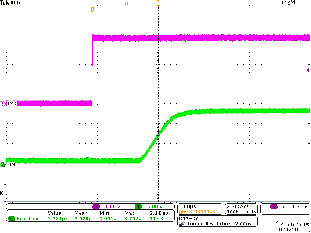
GUID-A14E45B8-FD99-4D5A-BF8E-F1ADA5AB3038-low.pngFigure 9-2 Dominant to Recessive Propagation Delay
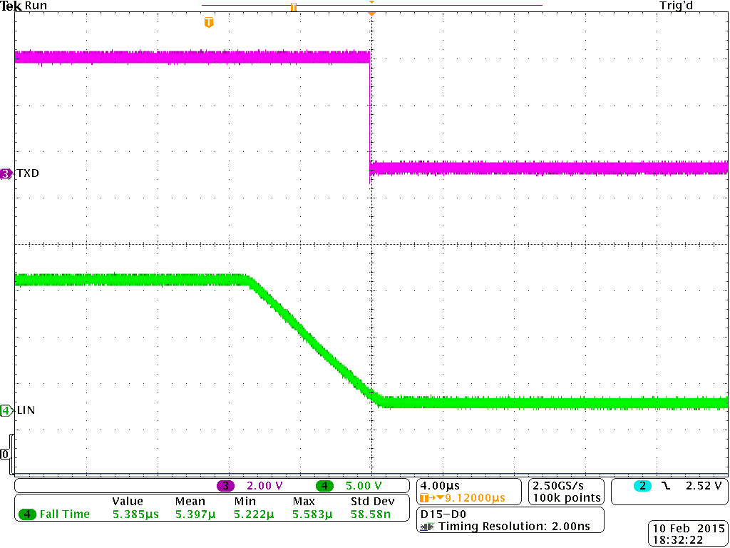
GUID-1D3D5E18-A95B-4050-8F26-0C532136AD1E-low.pngFigure 9-3 Recessive to Dominant Propagation Delay