SLVSDO6D August   2017  – December 2024 TPS1H000-Q1

PRODUCTION DATA  

  1.   1
  2. Features
  3. Applications
  4. Description
  5. Pin Configuration and Functions
  6. Specifications
    1. 5.1 Absolute Maximum Ratings
    2. 5.2 ESD Ratings
    3. 5.3 Recommended Operating Conditions
    4. 5.4 Thermal Information
    5. 5.5 Electrical Characteristics
    6. 5.6 Switching Characteristics
    7. 5.7 Typical Characteristics
  7. Detailed Description
    1. 6.1 Overview
    2. 6.2 Functional Block Diagram
    3. 6.3 Feature Description
      1. 6.3.1 Current Limit
      2. 6.3.2 DELAY Pin Configuration
        1. 6.3.2.1 Holding Mode
        2. 6.3.2.2 Latch-Off Mode
        3. 6.3.2.3 Auto-Retry Mode
      3. 6.3.3 Standalone Operation
      4. 6.3.4 Fault Truth Table
      5. 6.3.5 Full Diagnostics
        1. 6.3.5.1 Short-to-GND and Overload Detection
        2. 6.3.5.2 Open-Load Detection
          1. 6.3.5.2.1 Output On
          2. 6.3.5.2.2 Output Off
        3. 6.3.5.3 Short-to-Battery Detection
        4. 6.3.5.4 Thermal Fault Detection
          1. 6.3.5.4.1 Thermal Shutdown
          2. 6.3.5.4.2 Thermal Swing
          3. 6.3.5.4.3 Fault Report Holding
      6. 6.3.6 Full Protections
        1. 6.3.6.1 UVLO Protection
        2. 6.3.6.2 Inductive Load Switching Off Clamp
        3. 6.3.6.3 Loss-of-GND Protection
        4. 6.3.6.4 Loss-of-Power-Supply Protection
        5. 6.3.6.5 Reverse-Current Protection
        6. 6.3.6.6 MCU I/O Protection
    4. 6.4 Device Functional Modes
      1. 6.4.1 Working Modes
        1. 6.4.1.1 Normal Mode
        2. 6.4.1.2 Standby Mode
        3. 6.4.1.3 Standby Mode With Diagnostics
  8. Application and Implementation
    1. 7.1 Application Information
    2. 7.2 Typical Application
      1. 7.2.1 Design Requirements
      2. 7.2.2 Detailed Design Procedure
      3. 7.2.3 Application Curves
    3. 7.3 Power Supply Recommendations
    4. 7.4 Layout
      1. 7.4.1 Layout Guidelines
      2. 7.4.2 Layout Example
  9. Device and Documentation Support
    1. 8.1 Receiving Notification of Documentation Updates
    2. 8.2 Support Resources
    3. 8.3 Trademarks
    4. 8.4 Electrostatic Discharge Caution
    5. 8.5 Glossary
  10. Revision History
  11. 10Mechanical, Packaging, and Orderable Information

Package Options

Mechanical Data (Package|Pins)
Thermal pad, mechanical data (Package|Pins)
Orderable Information

Description

The TPS1H000-Q1 device is a fully protected single-channel high-side power switch with an integrated 1000mΩ NMOS power FET.

An adjustable current limit improves system reliability by limiting the inrush or overload current. The high accuracy of the current limit improves overload protection, simplifying the front-stage power design. Configurable features besides current limit provide design flexibility in the areas of functionality, cost, and thermal dissipation.

The device supports full diagnostics with the digital status output. Open-load detection is available in both the ON- and OFF-states. The device supports operation with or without an MCU. Standalone mode allows use of the device in isolated systems.

Package Information
PART NUMBER PACKAGE(1) PACKAGE SIZE(2)
TPS1H000-Q1 DGN (HVSSOP, 8) 3.00mm × 4.90mm
For all available packages, see the orderable addendum at the end of the data sheet.
The package size (length × width) is a nominal value and includes pins, where applicable.
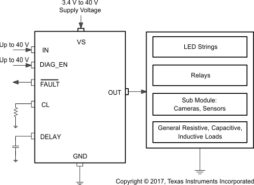
TPS1H000-Q1 Typical Block DiagramTypical Block Diagram
TPS1H000-Q1 Current-Limit Protection in
                        Auto-Retry ModeCurrent-Limit Protection in Auto-Retry Mode