SLVSCM2D October   2014  – December 2019 TPS1H100-Q1

PRODUCTION DATA.  

  1. Features
  2. Applications
  3. Description
    1.     Device Images
      1.      Typical Application Schematic
  4. Revision History
  5. Pin Configuration and Functions
    1.     Pin Functions
  6. Specifications
    1. 6.1 Absolute Maximum Ratings
    2. 6.2 ESD Ratings
    3. 6.3 Recommended Operating Conditions
    4. 6.4 Thermal Information
    5. 6.5 Electrical Characteristics
    6. 6.6 Timing Requirements – Current Sense Characteristics
    7. 6.7 Switching Characteristics
    8. 6.8 Typical Characteristics
  7. Detailed Description
    1. 7.1 Overview
    2. 7.2 Functional Block Diagram
    3. 7.3 Feature Description
      1. 7.3.1 Accurate Current Sense
      2. 7.3.2 Programmable Current Limit
      3. 7.3.3 Inductive-Load Switching-Off Clamp
      4. 7.3.4 Full Protections and Diagnostics
        1. 7.3.4.1  Short-to-GND and Overload Detection
        2. 7.3.4.2  Open-Load Detection
        3. 7.3.4.3  Short-to-Battery Detection
        4. 7.3.4.4  Reverse-Polarity Detection
        5. 7.3.4.5  Thermal Protection Behavior
        6. 7.3.4.6  UVLO Protection
        7. 7.3.4.7  Loss of GND Protection
        8. 7.3.4.8  Loss of Power Supply Protection
        9. 7.3.4.9  Reverse Current Protection
        10. 7.3.4.10 Protection for MCU I/Os
      5. 7.3.5 Diagnostic Enable Function
    4. 7.4 Device Functional Modes
      1. 7.4.1 Working Mode
  8. Application and Implementation
    1. 8.1 Application Information
    2. 8.2 Typical Application
      1. 8.2.1 Design Requirements
      2. 8.2.2 Detailed Design Procedure
        1. 8.2.2.1 Distinguishing of Different Fault Modes
        2. 8.2.2.2 AEC Q100-012 Test Grade A Certification
        3. 8.2.2.3 EMC Transient Disturbances Test
      3. 8.2.3 Application Curves
  9. Power Supply Recommendations
  10. 10Layout
    1. 10.1 Layout Guidelines
    2. 10.2 Layout Example
      1. 10.2.1 Without a GND Network
      2. 10.2.2 With a GND Network
    3. 10.3 Thermal Considerations
  11. 11Device and Documentation Support
    1. 11.1 Receiving Notification of Documentation Updates
    2. 11.2 Community Resources
    3. 11.3 Trademarks
    4. 11.4 Electrostatic Discharge Caution
    5. 11.5 Glossary
  12. 12Mechanical, Packaging, and Orderable Information

Package Options

Mechanical Data (Package|Pins)
Thermal pad, mechanical data (Package|Pins)
Orderable Information

Typical Characteristics

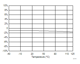
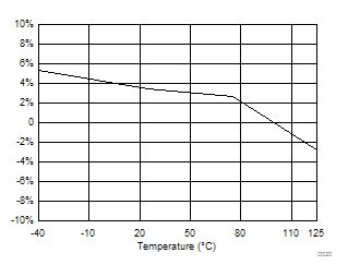
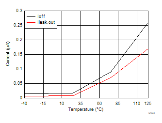
All the following data are based on the mean value of the three lots samples, VVS = 13.5 V if not specified.
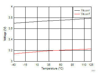
TPS1H100-Q1 D001_SLVSCM2.gif
Figure 8. VVS,UVR and VVS,UVF
TPS1H100-Q1 D003_SLVSCM2.gif
Figure 10. Ioff and Ileak,out
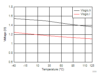
TPS1H100-Q1 D005_SLVSCM2.gif
Figure 12. Vlogic,h and Vlogic,l
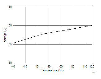
TPS1H100-Q1 D007_SLVSCM2.gif
Figure 14. VDS, clamp
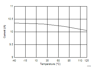
TPS1H100-Q1 D009_SLVSCM2.gif
Figure 16. Ilim,nom
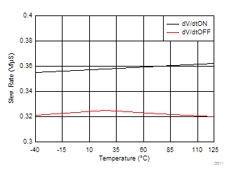
TPS1H100-Q1 D011_SLVSCM2.gif
Figure 18. dV/dtON and dV/dtOFF
TPS1H100-Q1 D013_SLVSCM2.gif
Figure 20. Vol,off
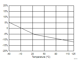
TPS1H100-Q1 D015_SLVSCM2.gif
Figure 22. KCS = 5 mA, 13.5 V
TPS1H100-Q1 D019_SLVSCM2.gif
Figure 24. KCS = 50 mA, 13.5 V
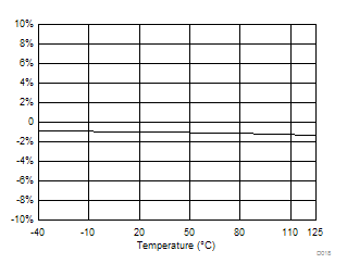
TPS1H100-Q1 D018_SLVSCM2.gif
Figure 26. KCS = 1 A, 13.5 V
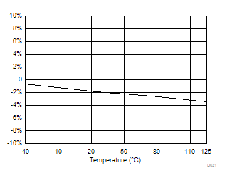
TPS1H100-Q1 D021_SLVSCM2.gif
Figure 28. KCL = 1.6 A, 13.5 V
TPS1H100-Q1 D002_SLVSCM2.gif
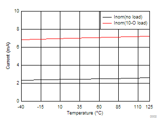
Figure 9. Inom With No Load and 10-Ω Load
TPS1H100-Q1 D004_SLVSCM2.gif
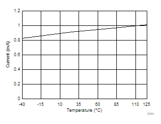
Figure 11. Ioff,diag
TPS1H100-Q1 D006_SLVSCM2.gif
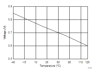
Figure 13. VF
TPS1H100-Q1 D008_SLVSCM2.gif
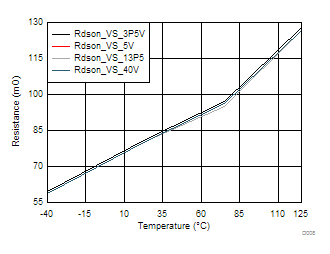
Figure 15. RDSON
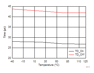
TPS1H100-Q1 D010_SLVSCM2.gif
Figure 17. TDon and TDoff
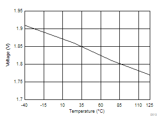
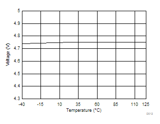
TPS1H100-Q1 D012_SLVSCM2.gif
Figure 19. VCS,h
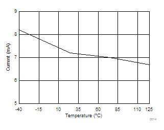
TPS1H100-Q1 D014_SLVSCM2.gif
Figure 21. Iol,on
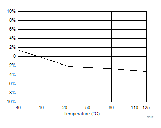
TPS1H100-Q1 D017_SLVSCM2.gif
Figure 23. KCS = 25 mA, 13.5 V
TPS1H100-Q1 D016_SLVSCM2.gif
Figure 25. KCS = 100 mA, 13.5 V
TPS1H100-Q1 D020_SLVSCM2.gif
Figure 27. KCL = 0.5 A, 13.5 V