SLVSE19B June   2019  – November 2021 TPS1HB50-Q1

PRODUCTION DATA  

  1. Features
  2. Applications
  3. Description
  4. Revision History
  5. Device Comparison Table
  6. Pin Configuration and Functions
    1. 6.1 Recommended Connections for Unused Pins
  7. Specifications
    1. 7.1 Absolute Maximum Ratings
    2. 7.2 ESD Ratings
    3. 7.3 Recommended Operating Conditions
    4. 7.4 Thermal Information
    5. 7.5 Electrical Characteristics
    6. 7.6 SNS Timing Characteristics
    7. 7.7 Switching Characteristics
    8. 7.8 Typical Characteristics
  8. Parameter Measurement Information
  9. Detailed Description
    1. 9.1 Overview
    2. 9.2 Functional Block Diagram
    3. 9.3 Feature Description
      1. 9.3.1 Protection Mechanisms
        1. 9.3.1.1 Thermal Shutdown
        2. 9.3.1.2 Current Limit
          1. 9.3.1.2.1 Current Limit Foldback
          2. 9.3.1.2.2 Programmable Current Limit
          3. 9.3.1.2.3 Undervoltage Lockout (UVLO)
          4. 9.3.1.2.4 VBB During Short-to-Ground
        3. 9.3.1.3 Voltage Transients
          1. 9.3.1.3.1 Load Dump
          2. 9.3.1.3.2 Driving Inductive Loads
        4. 9.3.1.4 Reverse Battery
        5. 9.3.1.5 Fault Event – Timing Diagrams
      2. 9.3.2 Diagnostic Mechanisms
        1. 9.3.2.1 VOUT Short-to-Battery and Open-Load
          1. 9.3.2.1.1 Detection With Switch Enabled
          2. 9.3.2.1.2 Detection With Switch Disabled
        2. 9.3.2.2 SNS Output
          1. 9.3.2.2.1 RSNS Value
            1. 9.3.2.2.1.1 High Accuracy Load Current Sense
            2. 9.3.2.2.1.2 SNS Output Filter
        3. 9.3.2.3 Fault Indication and SNS Mux
        4. 9.3.2.4 Resistor Sharing
        5. 9.3.2.5 High-Frequency, Low Duty-Cycle Current Sensing
    4. 9.4 Device Functional Modes
      1. 9.4.1 Off
      2. 9.4.2 Standby
      3. 9.4.3 Diagnostic
      4. 9.4.4 Standby Delay
      5. 9.4.5 Active
      6. 9.4.6 Fault
  10. 10Application and Implementation
    1. 10.1 Application Information
      1. 10.1.1 Ground Protection Network
      2. 10.1.2 Interface With Microcontroller
      3. 10.1.3 I/O Protection
      4. 10.1.4 Inverse Current
      5. 10.1.5 Loss of GND
      6. 10.1.6 Automotive Standards
        1. 10.1.6.1 ISO7637-2
        2. 10.1.6.2 AEC-Q100-012 Short Circuit Reliability
      7. 10.1.7 Thermal Information
    2. 10.2 Typical Application
      1. 10.2.1 Design Requirements
      2. 10.2.2 Detailed Design Procedure
        1. 10.2.2.1 Thermal Considerations
        2. 10.2.2.2 RILIM Calculation
        3. 10.2.2.3 Diagnostics
          1. 10.2.2.3.1 Selecting the RISNS Value
  11. 11Power Supply Recommendations
  12. 12Layout
    1. 12.1 Layout Guidelines
    2. 12.2 Layout Example
  13. 13Device and Documentation Support
    1. 13.1 Documentation Support
      1. 13.1.1 Related Documentation
    2. 13.2 Receiving Notification of Documentation Updates
    3. 13.3 Support Resources
    4. 13.4 Trademarks
    5. 13.5 Electrostatic Discharge Caution
    6. 13.6 Glossary
  14. 14Mechanical, Packaging, and Orderable Information

Package Options

Mechanical Data (Package|Pins)
Thermal pad, mechanical data (Package|Pins)
Orderable Information

Application Information

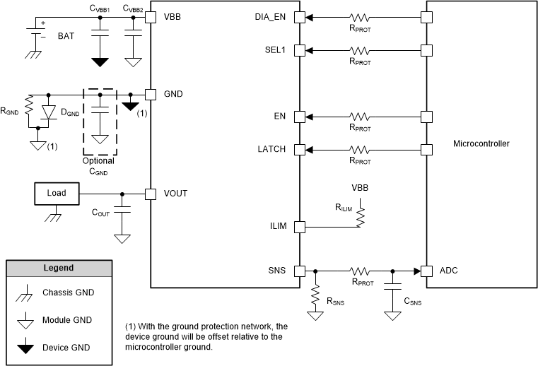
Figure 10-1 shows the schematic of a typical application of the TPS1HB50-Q1. It includes all standard external components. This section of the datasheet discusses the considerations in implementing commonly required application functionality.
GUID-AC60803B-3A59-4AC9-8BE2-5A201FC61461-low.gif
With the ground protection network, the device ground will be offset relative to the microcontroller ground.
Figure 10-1 System Diagram
Table 10-1 Recommended External Components
COMPONENTTYPICAL VALUEPURPOSE
RPROT15 kΩProtect microcontroller and device I/O pins.
RSNS1 kΩTranslate the sense current into sense voltage.
CSNS100 pF–10 nFLow-pass filter for the ADC input.
RGND4.7 kΩStabilize GND potential during turn-off of inductive load.
DGNDBAS21 DiodeProtects device during reverse battery.
RILIM5 kΩ–25 kΩ Set current limit threshold.
CVBB14.7 nF to Device GNDFiltering of voltage transients (for example, ESD, ISO7637-2) and improved emissions.
CVBB2220 nF to Module GNDStabilize the input supply and filter out low frequency noise.
COUT220 nFFiltering of voltage transients (for example, ESD, ISO7637-2).