SLVSFL4 June 2020 TPS2124
PRODUCTION DATA.
- 1 Features
- 2 Applications
- 3 Description
- 4 Revision History
- 5 Pin Configuration and Functions
- 6 Specifications
- 7 Parameter Measurement Information
-
8 Detailed Description
- 8.1 Overview
- 8.2 Functional Block Diagram
- 8.3 Feature Description
- 8.4 TPS2124 Device Functional Modes
- 9 Application and Implementation
- 10Power Supply Recommendations
- 11Layout
- 12Device and Documentation Support
- 13Mechanical, Packaging, and Orderable Information
Package Options
Mechanical Data (Package|Pins)
- YFP|20
Thermal pad, mechanical data (Package|Pins)
Orderable Information
9.4 Reverse Polarity Protection with TPS2124
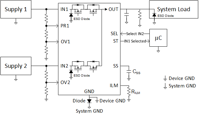
For applications that require reverse polarity protection, the TPS2124 can be configured to protect against mis-wiring input power supplies and block reverse current that could potentially damage the system. By connecting a diode on the GND pin of the TPS2124, this prevents reverse current from flowing back into the device when VIN is below system ground.
Since the TPS2124 has an absolute maximum rating of 24 V when referenced to device ground, the GND diode should be rated to standoff voltages up to the maximum reverse voltage. Furthermore, since the control pin voltages (PR1, OV1, OV2, etc.) are in reference to system GND, the voltage thresholds will need to be recalculated based on the voltage drop across the diode. To reduce the voltage drop, a resistor in parallel with the diode can also be used.
 Figure 21. TPS2124 Reverse Polarity Configuration