SLVSCO0E June 2014 – October 2020
PRODUCTION DATA
- 1 Features
- 2 Applications
- 3 Description
- 4 Revision History
- 5 Device Comparison Table
- 6 Pin Configuration and Functions
- 7 Specifications
- 8 Parameter Measurement Information
- 9 Detailed Description
- 10Application and Implementation
- 11Power Supply Recommendations
- 12Layout
- 13Device and Documentation Support
- 14Mechanical, Packaging, and Orderable Information
Package Options
Mechanical Data (Package|Pins)
- YFP|4
Thermal pad, mechanical data (Package|Pins)
Orderable Information
12.1.1 Thermal Considerations
For best performance, all traces must be as short as possible. To be most effective, the input and output capacitors must be placed close to the device to minimize the effects that parasitic trace inductances may have on normal and short-circuit operation. Using wide traces for VIN, VOUT, and GND helps minimize the parasitic electrical effects along with minimizing the case to ambient thermal impedance.
The maximum IC junction temperature must be restricted to 125°C under normal operating conditions. To calculate the maximum allowable dissipation, PD(max) for a given output current and ambient temperature, use Equation 3.
Equation 3. 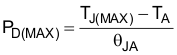
where
- PD(MAX) = maximum allowable power dissipation
- TJ(MAX) = maximum allowable junction temperature (125°C for the TPS22914/15)
- TA = ambient temperature of the device
- θJA = junction to air thermal impedance. Refer to the Thermal Information table. This parameter is highly dependent upon board layout.