SLVSDW8B September 2017 – December 2021 TPS22917
PRODUCTION DATA
- 1 Features
- 2 Applications
- 3 Description
- 4 Revision History
- 5 Device Comparison Table
- 6 Pin Configuration and Functions
- 7 Specifications
- 8 Parameter Measurement Information
- 9 Detailed Description
- 10Application and Implementation
- 11Power Supply Recommendations
- 12Layout
- 13Device and Documentation Support
- 14Mechanical, Packaging, and Orderable Information
Package Options
Mechanical Data (Package|Pins)
- DBV|6
Thermal pad, mechanical data (Package|Pins)
Orderable Information
12.3 Thermal Considerations
The maximum IC junction temperature must be restricted to 125°C under normal operating conditions. To calculate the maximum allowable dissipation, PD(max) for a given output current and ambient temperature, use Equation 12:
Equation 12. 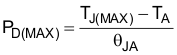
where
- PD(MAX) = maximum allowable power dissipation
- TJ(MAX) = maximum allowable junction temperature (125°C for the TPS22917x)
- TA = ambient temperature of the device
- θJA = junction to air thermal impedance. Refer to the Thermal Information section. This parameter is highly dependent upon board layout.