SLVSDW8B September 2017 – December 2021 TPS22917
PRODUCTION DATA
- 1 Features
- 2 Applications
- 3 Description
- 4 Revision History
- 5 Device Comparison Table
- 6 Pin Configuration and Functions
- 7 Specifications
- 8 Parameter Measurement Information
- 9 Detailed Description
- 10Application and Implementation
- 11Power Supply Recommendations
- 12Layout
- 13Device and Documentation Support
- 14Mechanical, Packaging, and Orderable Information
Package Options
Mechanical Data (Package|Pins)
- DBV|6
Thermal pad, mechanical data (Package|Pins)
Orderable Information
3 Description
The TPS22917x device is a small, single channel load switch using a low leakage P-Channel MOSFET for minimum power loss. Advanced gate control design supports operating voltages as low as 1 V with minimal increase in ON-Resistance and power loss.
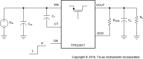
The Rise and Fall times can be independently adjusted with external components for system level optimizations. The timing capacitor (CT) and turn on time can be adjusted to manage inrush current without adding unnecessary system delays. The output discharge resistance (QOD) can be used to adjust the output fall time. Connect the QOD pin directly to the output for a fastest fall time or leave it open for the slowest fall time.
The switch ON state is controlled by a digital input that can interface directly with low-voltage control signals. The TPS22917 uses active high enable logic, while the TPS22917L uses active low. When power is first applied, a Smart Pulldown is used to keep the ON pin from floating until system sequencing is complete. After the ON pin is deliberately driven high (≥VIH), the Smart Pulldown (RPD) is disconnected to prevent unnecessary power loss.
The TPS22917x device is available in a leaded SOT-23 package (DBV) which allows visual inspection of solder joints. The device is characterized for operation over a temperature range of –40°C to 125°C.
| PART NUMBER | PACKAGE | BODY SIZE (NOM) |
|---|---|---|
| TPS22917x | SOT-23 (6) | 2.90 mm × 1.60 mm |
 Simplified Schematic