SLVSDW8B September 2017 – December 2021 TPS22917
PRODUCTION DATA
- 1 Features
- 2 Applications
- 3 Description
- 4 Revision History
- 5 Device Comparison Table
- 6 Pin Configuration and Functions
- 7 Specifications
- 8 Parameter Measurement Information
- 9 Detailed Description
- 10Application and Implementation
- 11Power Supply Recommendations
- 12Layout
- 13Device and Documentation Support
- 14Mechanical, Packaging, and Orderable Information
Package Options
Mechanical Data (Package|Pins)
- DBV|6
Thermal pad, mechanical data (Package|Pins)
Orderable Information
7.7.2 Typical Switching Characteristics
The typical data in this section apply at 25°C with a load of
CL = 1 μF, RL = 10 Ω, and QOD shorted to VOUT
unless otherwise noted.
The typical data in this section apply at 25°C with a load of
CL = 1 μF, RL = 10 Ω, and QOD shorted to VOUT
unless otherwise noted.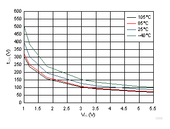 Figure 7-7 Turn-On Time (CT = Open). The typical data in this section apply at 25°C with a load of
CL = 1 μF, RL = 10 Ω, and QOD shorted to VOUT
unless otherwise noted.
 Figure 7-7 Turn-On Time (CT = Open). The typical data in this section apply at 25°C with a load of
CL = 1 μF, RL = 10 Ω, and QOD shorted to VOUT
unless otherwise noted.
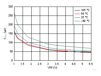 Figure 7-9 Rise
Time (CT = Open)
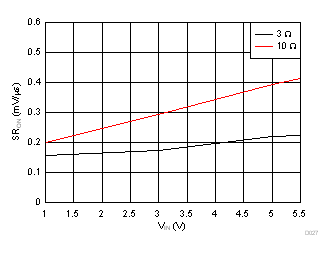
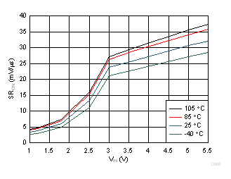 Figure 7-11 Slew
Rate (CT = Open)
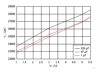
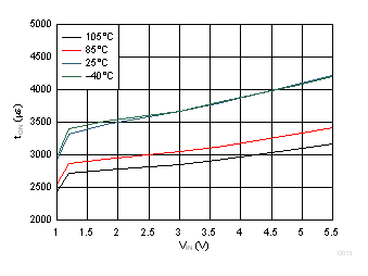 Figure 7-13 Turn
On Time (CT = 1000 pF)
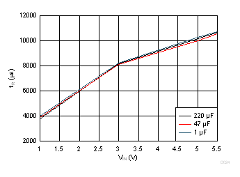
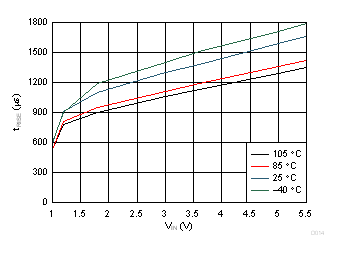 Figure 7-15 Rise
Time (CT = 1000 pF)
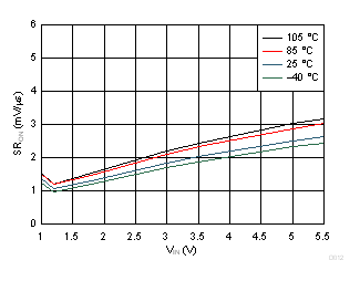 Figure 7-17 Slow
Slew Rate (CT = 1000 pF)
| RL = 10 Ω |
| RL = 10 Ω |
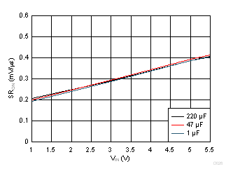
| RL = 10 Ω |
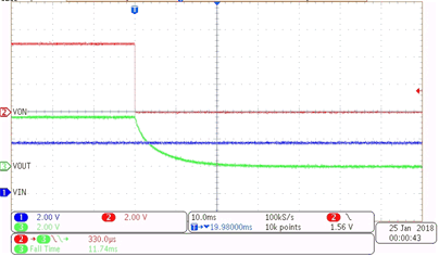
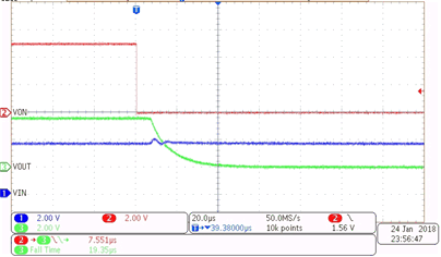 Figure 7-25 Turn-Off at 3.6 V
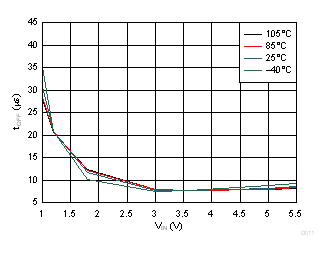
| VIN = 1 V to 5.5 V |
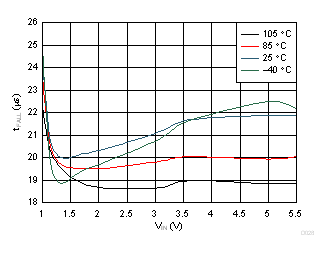
| VIN = 1 V to 5.5 V | ||||||
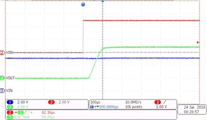 Figure 7-8 Turn-On at 5 V (CT = Open)
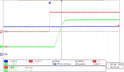 Figure 7-10 Turn-On at 3.6 V (CT =
Open)
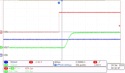 Figure 7-12 Turn On at 1 V (CT =
Open)
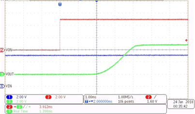 Figure 7-14 Turn-On at 5 V (CT = 1000 pF)
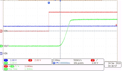 Figure 7-16 Turn-On at 3.6 V (CT = 1000 pF)
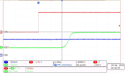 Figure 7-18 Turn-On at 1 V (CT = 1000 pF)
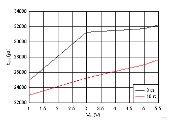
| CL = 47 µF |
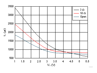
| CL = 47 µF |
| CL = 47 µF |
| RL = Open | CL = 47 μF | ||
| VIN = 1 V to 5.5 V | RL = Open |
| VIN = 1 V to 5.5 V | RL = Open | |||||