SLVSEN5B October   2018  – May 2019 TPS22919

PRODUCTION DATA.  

  1. Features
  2. Applications
  3. Description
    1.     Device Images
      1.      Simplified Schematic
  4. Revision History
  5. Pin Configuration and Functions
    1.     Pin Functions
  6. Specifications
    1. 6.1 Absolute Maximum Ratings
    2. 6.2 ESD Ratings
    3. 6.3 Recommended Operating Conditions
    4. 6.4 Thermal Information
    5. 6.5 Electrical Characteristics
    6. 6.6 Switching Characteristics
    7. 6.7 Typical Characteristics
  7. Parameter Measurement Information
    1. 7.1 Test Circuit and Timing Waveforms Diagrams
  8. Detailed Description
    1. 8.1 Overview
    2. 8.2 Functional Block Diagram
    3. 8.3 Feature Description
      1. 8.3.1 On and Off Control
      2. 8.3.2 Output Short Circuit Protection (ISC)
      3. 8.3.3 Fall Time (tFALL) and Quick Output Discharge (QOD)
        1. 8.3.3.1 QOD When System Power is Removed
    4. 8.4 Device Functional Modes
  9. Application and Implementation
    1. 9.1 Application Information
    2. 9.2 Typical Application
      1. 9.2.1 Design Requirements
      2. 9.2.2 Detailed Design Procedure
        1. 9.2.2.1 Limiting Inrush Current
        2. 9.2.2.2 Setting Fall Time for Shutdown Power Sequencing
        3. 9.2.2.3 Application Curves
  10. 10Power Supply Recommendations
  11. 11Layout
    1. 11.1 Layout Guidelines
    2. 11.2 Layout Example
    3. 11.3 Thermal Considerations
  12. 12Device and Documentation Support
    1. 12.1 Receiving Notification of Documentation Updates
    2. 12.2 Community Resources
    3. 12.3 Trademarks
    4. 12.4 Electrostatic Discharge Caution
    5. 12.5 Glossary
  13. 13Mechanical, Packaging, and Orderable Information

Package Options

Mechanical Data (Package|Pins)
Thermal pad, mechanical data (Package|Pins)
Orderable Information

Pin Configuration and Functions

DCK Package
6-Pin SC-70
Top View
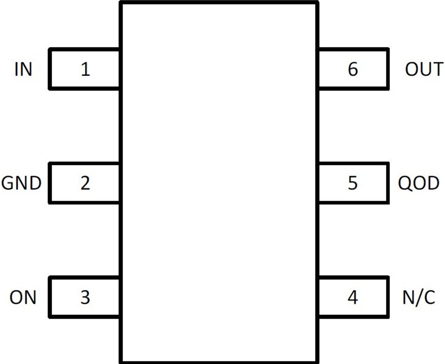
TPS22919 Pinout.png

Pin Functions

PIN I/O DESCRIPTION
NO. NAME
1 IN I Switch input.
2 GND Device ground.
3 ON I Active high switch control input. Do not leave floating.
4 NC No connect pin, leave floating.
5 QOD O Quick Output Discharge pin. This functionality can be enabled in one of three ways.
  • Placing an external resistor between VOUT and QOD
  • Tying QOD directly to VOUT and using the internal resistor value (RPD)
  • Disabling QOD by leaving pin floating
See the Fall Time (tFALL) and Quick Output Discharge (QOD) section for more information.
6 VOUT O Switch output.