SLVSGK4A November 2021 – June 2022 TPS22953-Q1 , TPS22954-Q1
PRODUCTION DATA
- 1 Features
- 2 Applications
- 3 Description
- 4 Revision History
- 5 Device Comparison Table
- 6 Pin Configuration and Functions
-
7 Specifications
- 7.1 Absolute Maximum Ratings
- 7.2 ESD Ratings
- Recommended Operating Conditions
- 7.3 Thermal Information
- 7.4 Electrical Characteristics
- 7.5 Electrical Characteristics – VBIAS = 5 V
- 7.6 Electrical Characteristics – VBIAS = 3.3 V
- 7.7 Electrical Characteristics – VBIAS = 2.5 V
- 7.8 Switching Characteristics – CT = 1000 pF
- 7.9 Switching Characteristics – CT = 0 pF
- 7.10 Typical DC Characteristics
- 7.11 Typical Switching Characteristics
- 8 Parameter Measurement Information
-
9 Detailed Description
- 9.1 Overview
- 9.2 Functional Block Diagram
- 9.3
Feature Description
- 9.3.1 On and Off Control (EN Pin)
- 9.3.2 Voltage Monitoring (SNS Pin)
- 9.3.3 Power Good (PG Pin)
- 9.3.4 Supervisor Fault Detection and Automatic Restart
- 9.3.5 Manual Restart
- 9.3.6 Thermal Shutdown
- 9.3.7 Reverse Current Blocking (TPS22953-Q1 Only)
- 9.3.8 Quick Output Discharge (QOD) (TPS22954-Q1 Only)
- 9.3.9 VIN and VBIAS Voltage Range
- 9.3.10 Adjustable Rise Time (CT Pin)
- 9.3.11 Power Sequencing
- 9.4 Device Functional Modes
- 10Application and Implementation
- 11Power Supply Recommendations
- 12Layout
- 13Device and Documentation Support
- 14Mechanical, Packaging, and Orderable Information
Package Options
Mechanical Data (Package|Pins)
- DQC|10
Thermal pad, mechanical data (Package|Pins)
- DQC|10
Orderable Information
9.3.1 On and Off Control (EN Pin)
The EN pin controls the state of the switch. When the voltage on EN exceeds VIH,EN the switch enables. When EN goes below VIL,EN the switch disables.
The EN pin has a blanking time of tBLANK on the rising edge after the VIH,EN threshold has been exceeded. The EN pin also has a de-glitch time of tDEGLITCH when the voltage has gone below VIL,EN.
The EN pin can also be configured through an external resistor divider to monitor a voltage signal for input UVLO. See Equation 1 and Figure 9-1 on how to configure the EN pin for input UVLO.
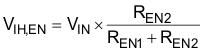
where
- VIH,EN is the rising threshold of the EN pin (see the Electrical Characteristics table)
- VIN is the input voltage being monitored (this can be VIN, VBIAS, or an external power supply)
- REN1, REN2 are the resistor divider values
") Figure 9-1 Resistor Divider (EN Pin)
Figure 9-1 Resistor Divider (EN Pin)