SLVSGK4A November 2021 – June 2022 TPS22953-Q1 , TPS22954-Q1
PRODUCTION DATA
- 1 Features
- 2 Applications
- 3 Description
- 4 Revision History
- 5 Device Comparison Table
- 6 Pin Configuration and Functions
-
7 Specifications
- 7.1 Absolute Maximum Ratings
- 7.2 ESD Ratings
- Recommended Operating Conditions
- 7.3 Thermal Information
- 7.4 Electrical Characteristics
- 7.5 Electrical Characteristics – VBIAS = 5 V
- 7.6 Electrical Characteristics – VBIAS = 3.3 V
- 7.7 Electrical Characteristics – VBIAS = 2.5 V
- 7.8 Switching Characteristics – CT = 1000 pF
- 7.9 Switching Characteristics – CT = 0 pF
- 7.10 Typical DC Characteristics
- 7.11 Typical Switching Characteristics
- 8 Parameter Measurement Information
-
9 Detailed Description
- 9.1 Overview
- 9.2 Functional Block Diagram
- 9.3
Feature Description
- 9.3.1 On and Off Control (EN Pin)
- 9.3.2 Voltage Monitoring (SNS Pin)
- 9.3.3 Power Good (PG Pin)
- 9.3.4 Supervisor Fault Detection and Automatic Restart
- 9.3.5 Manual Restart
- 9.3.6 Thermal Shutdown
- 9.3.7 Reverse Current Blocking (TPS22953-Q1 Only)
- 9.3.8 Quick Output Discharge (QOD) (TPS22954-Q1 Only)
- 9.3.9 VIN and VBIAS Voltage Range
- 9.3.10 Adjustable Rise Time (CT Pin)
- 9.3.11 Power Sequencing
- 9.4 Device Functional Modes
- 10Application and Implementation
- 11Power Supply Recommendations
- 12Layout
- 13Device and Documentation Support
- 14Mechanical, Packaging, and Orderable Information
Package Options
Mechanical Data (Package|Pins)
- DQC|10
Thermal pad, mechanical data (Package|Pins)
- DQC|10
Orderable Information
9.3.2 Voltage Monitoring (SNS Pin)
The SNS pin of the device can be used to monitor the output voltage of the device or another voltage rail. The pin can be configured with an external resistor divider to set the desired trip point for the voltage being monitored or be tied to OUT directly. If the voltage on the SNS pin exceeds VIH,SNS, the voltage being monitored on the SNS pin is considered to be valid high. The voltage on the SNS pin must be greater than VIH,SNS for at least tBLANK before PG is asserted high. If the voltage on the SNS pin goes below VIL,SNS, then the switch powers cycle (that is, the switch is disabled and re-enabled). For proper functionality of the device, this pin must not be left floating. If a resistor divider is not being used for voltage sensing, this pin can be tied directly to VOUT.
The SNS pin has a blanking time of tBLANK on the rising edge after the VIH,SNS threshold has been exceeded. The SNS pin has a de-glitch time of tDEGLITCH when the voltage has gone below VIL,SNS.
See Equation 2 and Figure 9-2 on how to configure the SNS pin for voltage monitoring.
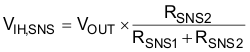
where
- VIH,SNS is the the rising threshold of the SNS pin (see Electrical Characteristics table)
- VOUT is the voltage on the OUTpin
- RSNS1, RSNS2 are the resistor divider values
") Figure 9-2 Voltage Divdier (SNS Pin)
Figure 9-2 Voltage Divdier (SNS Pin)