SLVSCI3E April   2014  – July 2022 TPS22965-Q1

PRODUCTION DATA  

  1. Features
  2. Applications
  3. Description
  4. Revision History
  5. Device Comparison Table
  6. Pin Configuration and Functions
  7. Specifications
    1. 7.1 Absolute Maximum Ratings
    2. 7.2 ESD Ratings
    3. 7.3 Recommended Operating Conditions
    4. 7.4 Thermal Information
    5. 7.5 Electrical Characteristics—VBIAS = 5 V
    6. 7.6 Electrical Characteristics—VBIAS = 2.5 V
    7. 7.7 Switching Characteristics
    8. 7.8 Typical Characteristics
      1. 7.8.1 Typical DC Characteristics
      2. 7.8.2 Typical Switching Characteristics
  8. Parameter Measurement Information
  9. Detailed Description
    1. 9.1 Overview
    2. 9.2 Functional Block Diagram
    3. 9.3 Feature Description
      1. 9.3.1 Adjustable Rise Time
      2. 9.3.2 Quick Output Discharge (TPS22965-Q1 and TPS22965W-Q1 Only)
      3. 9.3.3 Low Power Consumption During OFF State
    4. 9.4 Device Functional Modes
  10. 10Application and Implementation
    1. 10.1 Application Information
      1. 10.1.1 VIN to VOUT Voltage Drop
      2. 10.1.2 On and Off Control
      3. 10.1.3 Input Capacitor (Optional)
      4. 10.1.4 Output Capacitor (Optional)
      5. 10.1.5 VIN and VBIAS Voltage Range
    2. 10.2 Typical Application
      1. 10.2.1 Design Requirements
      2. 10.2.2 Detailed Design Procedure
        1. 10.2.2.1 Inrush Current
      3. 10.2.3 Application Curves
  11. 11Power Supply Recommendations
  12. 12Layout
    1. 12.1 Layout Guidelines
    2. 12.2 Layout Example
    3. 12.3 Thermal Consideration
  13. 13Device and Documentation Support
    1. 13.1 Documentation Support
      1. 13.1.1 Related Documentation
    2. 13.2 Receiving Notification of Documentation Updates
    3. 13.3 Support Resources
    4. 13.4 Trademarks
    5. 13.5 Electrostatic Discharge Caution
    6. 13.6 Glossary
  14. 14Mechanical, Packaging, and Orderable Information

Package Options

Mechanical Data (Package|Pins)
Thermal pad, mechanical data (Package|Pins)
Orderable Information

Thermal Consideration

The maximum IC junction temperature must be restricted to 150°C under normal operating conditions. Use the below equation as a guideline to calculate the maximum allowable dissipation, PD(max), for a given output current and ambient temperature.
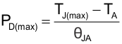
Equation 6. GUID-B5E3C346-67BB-40AB-BDC5-79552D941C7B-low.gif

where

  • PD(max) = maximum allowable power dissipation.
  • TJ(max) = maximum allowable junction temperature (150°C for the TPS22965x-Q1).
  • TA = ambient temperature of the device.
  • ΘJA = junction to air thermal impedance. See the Thermal Information table. This parameter is highly dependent upon board layout.

Refer to Figure 12-1. Notice the thermal vias located under the exposed thermal pad of the device. The thermal vias allow for thermal diffusion away from the device.