SLVSCG3F January   2014  – July 2017 TPS22968

PRODUCTION DATA.  

  1. Features
  2. Applications
  3. Description
    1.     Device Images
      1.      Typical Application Schematic
  4. Revision History
  5. Device Comparison
  6. Pin Configuration and Functions
    1.     Pin Functions
  7. Specifications
    1. 7.1 Absolute Maximum Ratings
    2. 7.2 ESD Ratings
    3. 7.3 Recommended Operating Conditions
    4. 7.4 Thermal Information
    5. 7.5 Electrical Characteristics (VBIAS = 5 V)
    6. 7.6 Electrical Characteristics (VBIAS = 2.5 V)
    7. 7.7 Switching Characteristics
    8. 7.8 Typical DC Characteristics
    9. 7.9 Typical AC Characteristics
  8. Parameter Measurement Information
  9. Detailed Description
    1. 9.1 Overview
    2. 9.2 Functional Block Diagram
    3. 9.3 Feature Description
      1. 9.3.1 ON and OFF Control
      2. 9.3.2 Input Capacitor (Optional)
      3. 9.3.3 Output Capacitor (Optional)
      4. 9.3.4 QOD (Optional)
      5. 9.3.5 VIN and VBIAS Voltage Range
      6. 9.3.6 Adjustable Rise Time
    4. 9.4 Device Functional Modes
  10. 10Application and Implementation
    1. 10.1 Application Information
      1. 10.1.1 Parallel Configuration
      2. 10.1.2 Standby Power Reduction
      3. 10.1.3 Power Supply Sequencing Without a GPIO Input
      4. 10.1.4 Reverse Current Blocking
    2. 10.2 Typical Application
      1. 10.2.1 Design Requirements
      2. 10.2.2 Detailed Design Procedure
        1. 10.2.2.1 VIN to VOUT Voltage Drop
        2. 10.2.2.2 Inrush Current
        3. 10.2.2.3 Thermal Considerations
      3. 10.2.3 Application Curves
  11. 11Power Supply Recommendations
  12. 12Layout
    1. 12.1 Layout Guidelines
    2. 12.2 Layout Example
  13. 13Device and Documentation Support
    1. 13.1 Device Support
      1. 13.1.1 Development Support
    2. 13.2 Documentation Support
      1. 13.2.1 Related Documentation
    3. 13.3 Related Links
    4. 13.4 Receiving Notification of Documentation Updates
    5. 13.5 Community Resources
    6. 13.6 Trademarks
    7. 13.7 Electrostatic Discharge Caution
    8. 13.8 Glossary
  14. 14Mechanical, Packaging, and Orderable Information

Package Options

Mechanical Data (Package|Pins)
Thermal pad, mechanical data (Package|Pins)
Orderable Information

VIN and VBIAS Voltage Range

For optimal RON performance, make sure VIN ≤ VBIAS. The device is still functional if VIN > VBIAS, but it exhibits RON greater than what is listed in the Electrical Characteristics (VBIAS = 5 V) and Electrical Characteristics (VBIAS = 2.5 V) table. See Figure 30 for an example of a typical device. Notice the increasing RON as VIN exceeds VBIAS voltage. Be sure to never exceed the maximum voltage rating for VIN and VBIAS.
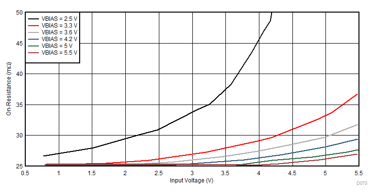
TPS22968 TPS22968N D070_SLVSCG3.gif
Temperature = 25°C IOUT = 200 mA
Figure 30. On-Resistance vs Input Voltage