SLVSDE7D November 2016 – December 2023 TPS22976
PRODUCTION DATA
- 1
- 1 Features
- 2 Applications
- 3 Description
- 4 Device Comparison Table
- 5 Pin Configuration and Functions
-
6 Specifications
- 6.1 Absolute Maximum Ratings
- 6.2 ESD Ratings
- 6.3 Recommended Operating Conditions
- 6.4 Thermal Information
- 6.5 Electrical Characteristics (VBIAS = 5V)
- 6.6 Electrical Characteristics (VBIAS = 2.5V)
- 6.7 Switching Characteristics (TPS22976)
- 6.8 Switching Characteristics (TPS22976A)
- 6.9 Switching Characteristics (TPS22976N)
- 6.10 Typical DC Characteristics
- 6.11 Typical AC Characteristics
- 7 Parameter Measurement Information
- 8 Detailed Description
- 9 Application and Implementation
- 10Device and Documentation Support
- 11Revision History
- 12Mechanical, Packaging, and Orderable Information
Package Options
Refer to the PDF data sheet for device specific package drawings
Mechanical Data (Package|Pins)
- DPU|14
Thermal pad, mechanical data (Package|Pins)
- DPU|14
Orderable Information
3 Description
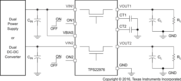
The TPS22976 product family consists of three devices: TPS22976, TPS22976A and TPS22976N. Each device is a dual-channel load switch with controlled turnon. The device contains two N-channel MOSFETs that can operate over an input voltage range of 0.6 V to 5.7 V, and can support a maximum continuous current of 6 A per channel. Each switch is independently controlled by an on and off input (ON1 and ON2), which can interface directly with low-voltage control signals. The TPS22976 is capable of thermal shutdown when the junction temperature is above the threshold, turning the switch off. The switch turns on again when the junction temperature stabilizes to a safe range. The TPS22976 also offers an optional integrated 230-Ω on-chip load resistor for quick output discharge when the switch is turned off.
The TPS22976 is available in a small, space-saving 3-mm × 2-mm 14-SON package (DPU) with integrated thermal pad allowing for high power dissipation. The device is characterized for operation over the free-air temperature range of –40°C to 105°C.
| PART NUMBER | PACKAGE | BODY SIZE (NOM) |
|---|---|---|
| TPS22976 TPS22976A TPS22976N | WSON (14) | 3.00 mm × 2.00 mm |
 Application Circuit