SLUSCD1C June 2017 – November 2018 TPS2373
PRODUCTION DATA.
- 1 Features
- 2 Applications
- 3 Description
- 4 Revision History
- 5 Pin Configuration and Functions
- 6 Specifications
-
7 Detailed Description
- 7.1 Overview
- 7.2 Functional Block Diagram
- 7.3
Feature Description
- 7.3.1 APD Auxiliary Power Detect
- 7.3.2 PG Power Good (Converter Enable) Pin Interface
- 7.3.3 CLSA and CLSB Classification
- 7.3.4 DEN Detection and Enable
- 7.3.5 Internal Pass MOSFET
- 7.3.6 TPH, TPL and BT PSE Type Indicators
- 7.3.7 VC_IN, VC_OUT, UVLO_SEL, and Advanced PWM Startup
- 7.3.8 AMPS_CTL, MPS_DUTY and Automatic MPS
- 7.3.9 VDD Supply Voltage
- 7.3.10 VSS
- 7.3.11 Exposed Thermal PAD
- 7.4
Device Functional Modes
- 7.4.1 PoE Overview
- 7.4.2 Threshold Voltages
- 7.4.3 PoE Startup Sequence
- 7.4.4 Detection
- 7.4.5 Hardware Classification
- 7.4.6 Inrush and Startup
- 7.4.7 Maintain Power Signature
- 7.4.8 Advanced Startup and Converter Operation
- 7.4.9 PD Hotswap Operation
- 7.4.10 Startup and Power Management, PG and TPH, TPL, BT
- 7.4.11 Adapter ORing
- 7.4.12 Using DEN to Disable PoE
- 7.4.13 ORing Challenges
-
8 Application and Implementation
- 8.1 Application Information
- 8.2
Typical Application
- 8.2.1 Design Requirements
- 8.2.2
Detailed Design Requirements
- 8.2.2.1 Input Bridges and Schottky Diodes
- 8.2.2.2 Protection, D1
- 8.2.2.3 Capacitor, C1
- 8.2.2.4 Detection Resistor, RDEN
- 8.2.2.5 Classification Resistors, RCLSA and RCLSB
- 8.2.2.6 APD Pin Divider Network RAPD1, RAPD2
- 8.2.2.7 Opto-isolators for TPH, TPL and BT
- 8.2.2.8 VC Input and Output, CVCIN and CVCOUT
- 8.2.2.9 UVLO Select, UVLO_SEL
- 8.2.2.10 Automatic MPS and MPS Duty Cycle, RMPS and RMPS_DUTY
- 8.2.2.11 Internal Voltage Reference, RREF
- 8.2.3 Application Curves
- 9 Power Supply Recommendations
- 10Layout
- 11Device and Documentation Support
- 12Mechanical, Packaging, and Orderable Information
Package Options
Refer to the PDF data sheet for device specific package drawings
Mechanical Data (Package|Pins)
- RGW|20
Thermal pad, mechanical data (Package|Pins)
Orderable Information
8.2.2.7 Opto-isolators for TPH, TPL and BT
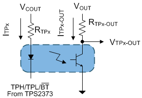
The TPH, TPL and BT pin are active-low, open-drain outputs, which give an indication about the PSE allocated power along with its Type. Optocouplers can interface these pins to circuitry on the secondary side of the converter. A high-gain optocoupler and a high-impedance (for example, CMOS) receiver are recommended. Design of the optocoupler interface can be accomplished as follows:
- As shown in Figure 31, let VCOUT = 12 V, VOUT = 5 V, RTPx–OUT = 10 kΩ, VTPx = 260 mV, VTPx-OUT = 400 mV.
- The optocoupler current transfer ratio, CTR, is needed to determine RTPx. A device with a minimum CTR of 100% at 1 mA LED bias current, ITPx, is selected. In practice, CTR will vary with temperature, LED bias current, and aging, These variations may require some iteration using the CTR-versus-IDIODE curve on the optocoupler data sheet.
- The approximate forward voltage of the optocoupler diode, VFWLED, is 1.1 V from the data sheet.
- Use Equation 5.
- Choose a 10.7 kΩ resistor.
Equation 5.

Most applications require that only the PSE’s allocated power information (TPH and TPL) is needed for the MCU or PD load. In this case, the circuitry needed to drive the BT signal is not necessary and the BT pin can be left floating.
Some applications such as PoE lighting can benefit from the BT signal to show that the power consumption in standby operation may not meet regulatory requirements. In non-standard PoE applications, BT is used with TPH and TPL to indicate a PoE++ PSE.
