SLVSER8A June 2020 – September 2020 TPS23734
PRODUCTION DATA
- 1 Features
- 2 Applications
- 3 Description
- 4 Revision History
- 5 Device Comparison Table
- 6 Pin Configuration and Functions
- 7 Specifications
-
8 Detailed Description
- 8.1 Overview
- 8.2 Functional Block Diagram
- 8.3
Feature Description
- 8.3.1 CLS Classification
- 8.3.2 DEN Detection and Enable
- 8.3.3 APD Auxiliary Power Detect
- 8.3.4 Internal Pass MOSFET
- 8.3.5 T2P and APDO Indicators
- 8.3.6
DC-DC Controller Features
- 8.3.6.1 VCC, VB, VBG and Advanced PWM Startup
- 28
- 8.3.6.2 CS, Current Slope Compensation and blanking
- 8.3.6.3 COMP, FB, EA_DIS, CP, PSRS and Opto-less Feedback
- 8.3.6.4 FRS Frequency Setting and Synchronization
- 8.3.6.5 DTHR and Frequency Dithering for Spread Spectrum Applications
- 8.3.6.6 SST and Soft-Start of the Switcher
- 8.3.6.7 SST, I_STP, LINEUV and Soft-Stop of the Switcher
- 8.3.7 Switching FET Driver - GATE, GTA2, DT
- 8.3.8 EMPS and Automatic MPS
- 8.3.9 VDD Supply Voltage
- 8.3.10 RTN, AGND, GND
- 8.3.11 VSS
- 8.3.12 Exposed Thermal pads - PAD_G and PAD_S
- 8.4
Device Functional Modes
- 8.4.1 PoE Overview
- 8.4.2 Threshold Voltages
- 8.4.3 PoE Start-Up Sequence
- 8.4.4 Detection
- 8.4.5 Hardware Classification
- 8.4.6 Maintain Power Signature (MPS)
- 8.4.7 Advanced Start-Up and Converter Operation
- 8.4.8 Line Undervoltage Protection and Converter Operation
- 8.4.9 PD Self-Protection
- 8.4.10 Thermal Shutdown - DC-DC Controller
- 8.4.11 Adapter ORing
-
9 Application and Implementation
- 9.1 Application Information
- 9.2
Typical Application
- 9.2.1
Design Requirements
- 9.2.1.1
Detailed Design Procedure
- 9.2.1.1.1 Input Bridges and Schottky Diodes
- 9.2.1.1.2 Input TVS Protection
- 9.2.1.1.3 Input Bypass Capacitor
- 9.2.1.1.4 Detection Resistor, RDEN
- 9.2.1.1.5 Classification Resistor, RCLS.
- 9.2.1.1.6 Dead Time Resistor, RDT
- 9.2.1.1.7 APD Pin Divider Network, RAPD1, RAPD2
- 9.2.1.1.8 Setting Frequency (RFRS) and Synchronization
- 9.2.1.1.9 Bias Supply Requirements and CVCC
- 9.2.1.1.10 APDO, T2P Interface
- 9.2.1.1.11 Secondary Soft Start
- 9.2.1.1.12 Frequency Dithering for Conducted Emissions Control
- 9.2.1.1
Detailed Design Procedure
- 9.2.1
Design Requirements
- 10Power Supply Recommendations
- 11Layout
- 12Device and Documentation Support
- 13Mechanical, Packaging, and Orderable Information
Package Options
Mechanical Data (Package|Pins)
- RMT|45
Thermal pad, mechanical data (Package|Pins)
Orderable Information
8.4.8 Line Undervoltage Protection and Converter Operation
When the input power source is removed, there are circumstances where stress may occur on the power components. For example with ACF topology, as VVDD-RTN gradually decreases the converter's operating duty cycle must compensate for the lower input voltage. At minimum input voltage the duty cycle nears its maximum value (DMAX), and the voltage across the clamp capacitor approaches its highest value since the transformer must be reset in a relatively short time. This results in potentially damaging overvoltage and oscillations. Also during next power up, due to precharged clamp capacitor, the soft-start could cause transformer saturation.
There are also situations where the output voltage capacitor may be able to back drive its secondary-side sync MOSFET(s) after the converter switching has stopped completely, either temporarily or not. Such situation could apply to both ACF and flyback (at power down or next soft-start) configurations.
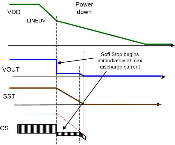
To address this case, once the LINEUV voltage falls below VLIUVF, the TPS23734 transitions to soft-stop mode. It turns on temporarily the startup to maintain VVCC, then uses the SST control to ramp down the switching MOSFET peak current. As a result, the converter output is discharged in a controlled way, the energy of the output capacitor being sent back to the input bulk capacitor. Also note that at beginning of soft-stop, the TPS23734 temporarily forces the peak current to a low value (VCS maximum at approximately 50 mV), until SST voltage becomes low enough to decrease it further. This advanced feature allows the soft-stop to immediately start discharging the output capacitor, regardless of the output load level, minimizing any system tradeoffs for optimum switching MOSFETs protection. See Figure 8-13.
 Figure 8-13 Soft-Stop Operation
Once the soft-stop operation has been completed and to avoid subsequent oscillations caused by the impact of the energy transfer on the LINEUV voltage, an internal load (~7 mA) is applied on VDD for approximately 160 ms, before the converter is allowed to restart.