SLVSB97E July 2012 – January 2018 TPS23751 , TPS23752
PRODUCTION DATA.
- 1 Features
- 2 Applications
- 3 Description
- 4 Revision History
- 5 Pin Configuration and Functions
-
6 Specifications
- 6.1 Absolute Maximum Ratings
- 6.2 ESD Ratings
- 6.3 ESD Ratings: Surge
- 6.4 Recommended Operating Conditions
- 6.5 Thermal Information
- 6.6 Electric Characteristics - Controller Section
- 6.7 Electrical Characteristics - Sleep Mode (TPS23752 Only)
- 6.8 Electrical Characteristics - PoE Interface Section
- 6.9 Typical Characteristics
-
7 Detailed Description
- 7.1 Overview
- 7.2 Functional Block Diagrams
- 7.3 Feature Description
- 7.4
Device Functional Modes
- 7.4.1 PoE Overview
- 7.4.2
Sleep Mode Operation (TPS23752 only)
- 7.4.2.1 Converter Controller Features
- 7.4.2.2 PWM and VFO Operation; CTL, SRT, and SRD Pin Relationships to Output Load Current
- 7.4.2.3 Bootstrap Topology
- 7.4.2.4 Current Slope Compensation and Current Limit
- 7.4.2.5 RT
- 7.4.2.6 T2P, Startup and Power Management
- 7.4.2.7 Thermal Shutdown
- 7.4.2.8 Adapter ORing
- 7.4.2.9 Using DEN to Disable PoE
- 7.4.2.10 ORing Challenges
-
8 Application and Implementation
- 8.1 Application Information
- 8.2
Typical Application
- 8.2.1 Design Requirements
- 8.2.2
Detailed Design Procedure
- 8.2.2.1 Input Bridges and Schottky Diodes
- 8.2.2.2 Protection, D1
- 8.2.2.3 Capacitor, C1
- 8.2.2.4 Detection Resistor, RDEN
- 8.2.2.5 Classification Resistor, RCLS
- 8.2.2.6 APD Pin Divider Network, RAPD1, RAPD2
- 8.2.2.7 Setting the PWM-VFO Threshold using the SRT pin
- 8.2.2.8 Setting Frequency (RT)
- 8.2.2.9 Current Slope Compensation
- 8.2.2.10 Voltage Feed-Forward Compensation
- 8.2.2.11 Estimating Bias Supply Requirements and Cvc
- 8.2.2.12 Switching Transformer Considerations and RVC
- 8.2.2.13 T2P Pin Interface
- 8.2.2.14 Softstart
- 8.2.2.15 Special Switching MOSFET Considerations
- 8.2.2.16 ESD
- 8.2.2.17 Thermal Considerations and OTSD
- 8.2.3 Application Curves
- 9 Power Supply Recommendations
- 10Layout
- 11Device and Documentation Support
- 12Mechanical, Packaging, and Orderable Information
Package Options
Mechanical Data (Package|Pins)
- PWP|16
Thermal pad, mechanical data (Package|Pins)
- PWP|16
Orderable Information
7.4.2.2 PWM and VFO Operation; CTL, SRT, and SRD Pin Relationships to Output Load Current
As the TPS23751 and TPS23752 transition from PWM to VFO mode with decreasing output load current, several things happen to help reduce the light load losses of the DC-DC converter. A summary is shown in Table 3.
Table 3. Comparison of PWM and VFO Modes
| MODE | SWITCHING FREQUENCY | INDUCTOR Peak CURRENT | SYNCHRONOUS RECTIFIER (control with SRD pin) | INTERNAL SLOPE COMPENSATION |
|---|---|---|---|---|
| PWM | Constant; set by RT | Variable, set by VCTL | Enabled (SRD = LOW) | Enabled |
| VFO | Variable; set by VCTL | Constant, clamped by VSRT | Disabled (SRD = OPEN) | Disabled |
The state of the SRD pin depends on the internal operating mode (PWM or VFO) and is used to enable or disable the synchronous rectifier. In addition to disabling the synchronous rectifier, the TPS23751 and TPS23752 reduce the switching frequency in VFO mode to maintain output regulation.
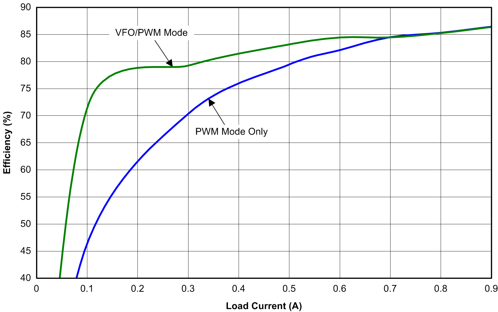
Synchronous rectification provides an efficiency advantage over a standard diode rectifier at medium to heavy loads, but not at lighter loads. The SRD feature can provide a means to recover the light load losses by disabling the synchronous rectifier and allowing the standard diode rectifier to take over as illustrated in Figure 28 by the VFO/PWM mode efficiency curve.
 Figure 28. TPS23751 and TPS23752 Light Load Efficiency versus Mode
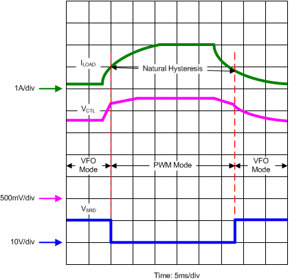
Figure 29 illustrates operation through the VFO to PWM to VFO transitions. As load current increases, so does VCTL. When VCTL exceeds the rising threshold, the TPS23751 and TPS23752 transition from VFO to PWM mode, and SRD goes low. The converter now operates with fixed frequency and current demand set by VCTL. As load current decreases, so does VCTL. When VCTL decays below the falling threshold, the TPS23751 and TPS23752 transition from PWM to VFO mode, and SRD goes high. The converter now operates with variable frequency set by VCTL, and fixed current demand set by VSRT.
 Figure 29. Converter Mode Transition
There is a natural load current hysteresis for ILOAD which can be seen in Figure 29 between the transition points. For increasing ILOAD, the transition current is slightly higher than for decreasing ILOAD. This condition is due partially to CTL pin hysteresis (approximately 35mV) and partially due to CTL pin operating point versus mode. VCTL is slightly higher in PWM mode than in VFO mode for given output load at or near the transition point.