SLVSB97E July 2012 – January 2018 TPS23751 , TPS23752
PRODUCTION DATA.
- 1 Features
- 2 Applications
- 3 Description
- 4 Revision History
- 5 Pin Configuration and Functions
-
6 Specifications
- 6.1 Absolute Maximum Ratings
- 6.2 ESD Ratings
- 6.3 ESD Ratings: Surge
- 6.4 Recommended Operating Conditions
- 6.5 Thermal Information
- 6.6 Electric Characteristics - Controller Section
- 6.7 Electrical Characteristics - Sleep Mode (TPS23752 Only)
- 6.8 Electrical Characteristics - PoE Interface Section
- 6.9 Typical Characteristics
-
7 Detailed Description
- 7.1 Overview
- 7.2 Functional Block Diagrams
- 7.3 Feature Description
- 7.4
Device Functional Modes
- 7.4.1 PoE Overview
- 7.4.2
Sleep Mode Operation (TPS23752 only)
- 7.4.2.1 Converter Controller Features
- 7.4.2.2 PWM and VFO Operation; CTL, SRT, and SRD Pin Relationships to Output Load Current
- 7.4.2.3 Bootstrap Topology
- 7.4.2.4 Current Slope Compensation and Current Limit
- 7.4.2.5 RT
- 7.4.2.6 T2P, Startup and Power Management
- 7.4.2.7 Thermal Shutdown
- 7.4.2.8 Adapter ORing
- 7.4.2.9 Using DEN to Disable PoE
- 7.4.2.10 ORing Challenges
-
8 Application and Implementation
- 8.1 Application Information
- 8.2
Typical Application
- 8.2.1 Design Requirements
- 8.2.2
Detailed Design Procedure
- 8.2.2.1 Input Bridges and Schottky Diodes
- 8.2.2.2 Protection, D1
- 8.2.2.3 Capacitor, C1
- 8.2.2.4 Detection Resistor, RDEN
- 8.2.2.5 Classification Resistor, RCLS
- 8.2.2.6 APD Pin Divider Network, RAPD1, RAPD2
- 8.2.2.7 Setting the PWM-VFO Threshold using the SRT pin
- 8.2.2.8 Setting Frequency (RT)
- 8.2.2.9 Current Slope Compensation
- 8.2.2.10 Voltage Feed-Forward Compensation
- 8.2.2.11 Estimating Bias Supply Requirements and Cvc
- 8.2.2.12 Switching Transformer Considerations and RVC
- 8.2.2.13 T2P Pin Interface
- 8.2.2.14 Softstart
- 8.2.2.15 Special Switching MOSFET Considerations
- 8.2.2.16 ESD
- 8.2.2.17 Thermal Considerations and OTSD
- 8.2.3 Application Curves
- 9 Power Supply Recommendations
- 10Layout
- 11Device and Documentation Support
- 12Mechanical, Packaging, and Orderable Information
Package Options
Mechanical Data (Package|Pins)
- PWP|20
Thermal pad, mechanical data (Package|Pins)
- PWP|20
Orderable Information
7.4.1.7 Startup and Converter Operation
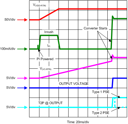
The internal PoE UVLO (Under Voltage Lock Out) circuit holds the hotswap switch off before the PSE provides full voltage to the PD. This prevents the converter circuits from loading the PoE input during detection and classification. The converter circuits discharge CIN, Cvc, and Cvb while the PD is unpowered. Thus V(VDD-RTN) is a small voltage just after applying full voltage to the PD, as seen in Figure 24. The PSE drives the PI voltage to the operating range once the PSE has decided to power up the PD. When VVDD rises above the UVLO turn-on threshold (VUVLO-R, approximately 38 V) with RTN high, the TPS23751 and TPS23752 enable the hotswap MOSFET with approximately 140 mA (inrush) current limit as seen in Figure 26. Converter switching is disabled while CIN charges and VRTN falls from VVDD to nearly VVSS, however the converter startup circuit is allowed to charge CVC (the bootstrap startup capacitor). Converter switching is allowed if the PD is not in inrush, OTSD is not active, and the VC UVLO permits it. Once the inrush current falls about 10% below the inrush current limit, the PD current limit switches to the operational level (approximately 1000 mA). Continuing the startup sequence shown in Figure 26, VVC continues to rise until the startup threshold (VCUV approximately 8.9 V) is exceeded, turning the startup source off and enabling switching. The VB regulator is always active, powering the internal converter circuits as VVC rises. There is a slight delay between the removal of charge current and the start of switching as the softstart ramp sweeps above the VZDC threshold. VVC falls as it powers both the internal circuits and the switching MOSFET gates. If the converter control bias output rises to support VVC before it falls to VCUV – VCUVH (approximately 5.7 V), a successful startup occurs. In Figure 26, T2P is active if a type 2 PSE is plugged in.
 Figure 26. Power Up and Start
 If VVDD- VVSS drops below the lower PoE UVLO (VUVLO-R - VUVLO-H, approximately 32 V), the hotswap MOSFET is turned off, but the converter still runs. The converter stops if VVC falls below the converter UVLO (VCUV – VCUVH, approximately 5.7 V), the hotswap is in inrush current limit, 0% duty cycle is demanded by VCTL (VCTL < VZDC, approximately 1.75 V), or the converter is in thermal shutdown.