SLVS933D July 2009 – December 2020 TPS23753A
PRODUCTION DATA
- 1 Features
- 2 Applications
- 3 Description
- 4 Revision History
- 5 Product Information
- 6 Pin Configuration and Functions
- 7 Specifications
-
8 Detailed Description
- 8.1 Overview
- 8.2 Functional Block Diagram
- 8.3 Feature Description
- 8.4
Device Functional Modes
- 8.4.1 Threshold Voltages
- 8.4.2 PoE Start-Up Sequence
- 8.4.3 Detection
- 8.4.4 Hardware Classification
- 8.4.5 Maintain Power Signature (MPS)
- 8.4.6 TPS23753A Operation
- 8.4.7 Special Switching MOSFET Considerations
- 8.4.8 Thermal Considerations
- 8.4.9 FRS and Synchronization
- 8.4.10 Blanking – RBLNK
- 8.4.11 Current Slope Compensation
- 8.4.12 Adapter ORing
- 8.4.13 Protection
- 8.4.14 Frequency Dithering for Conducted Emissions Control
- 9 Application and Implementation
- 10Power Supply Recommendations
- 11Layout
- 12Device and Documentation Support
- 13Mechanical, Packaging, and Orderable Information
Package Options
Mechanical Data (Package|Pins)
- PW|14
Thermal pad, mechanical data (Package|Pins)
Orderable Information
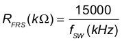
8.4.9 FRS and Synchronization
The FRS pin programs the (free-running) oscillator frequency, and may also be used to synchronize the TPS23753A converter to a higher frequency. The internal oscillator sets the maximum duty cycle and controls the current-compensation ramp circuit, making the ramp height independent of frequency. RFRS must be selected per Equation 5.
The TPS23753A may be synchronized to an external clock to eliminate beat frequencies from a sampled system, or to place emission spectrum away from an RF input frequency. Synchronization may be accomplished by applying a short pulse ( > 25 ns) of magnitude VSYNC to FRS as shown in Figure 8-7. RFRS must be chosen so that the maximum free-running frequency is just below the desired synchronization frequency. The synchronization pulse terminates the potential ON-time period, and the OFF-time period does not begin until the pulse terminates. A short pulse is preferred to avoid reducing the potential ON-time.
Figure 8-7 shows examples of nonisolated and transformer-coupled synchronization circuits RT reduces noise susceptibility for the isolation transformer implementation. The FRS node must be protected from noise because it is high impedance.
 Figure 8-7 Synchronization