SLVS933D July 2009 – December 2020 TPS23753A
PRODUCTION DATA
- 1 Features
- 2 Applications
- 3 Description
- 4 Revision History
- 5 Product Information
- 6 Pin Configuration and Functions
- 7 Specifications
-
8 Detailed Description
- 8.1 Overview
- 8.2 Functional Block Diagram
- 8.3 Feature Description
- 8.4
Device Functional Modes
- 8.4.1 Threshold Voltages
- 8.4.2 PoE Start-Up Sequence
- 8.4.3 Detection
- 8.4.4 Hardware Classification
- 8.4.5 Maintain Power Signature (MPS)
- 8.4.6 TPS23753A Operation
- 8.4.7 Special Switching MOSFET Considerations
- 8.4.8 Thermal Considerations
- 8.4.9 FRS and Synchronization
- 8.4.10 Blanking – RBLNK
- 8.4.11 Current Slope Compensation
- 8.4.12 Adapter ORing
- 8.4.13 Protection
- 8.4.14 Frequency Dithering for Conducted Emissions Control
- 9 Application and Implementation
- 10Power Supply Recommendations
- 11Layout
- 12Device and Documentation Support
- 13Mechanical, Packaging, and Orderable Information
Package Options
Mechanical Data (Package|Pins)
- PW|14
Thermal pad, mechanical data (Package|Pins)
- PW|14
Orderable Information
8.4.6.2 PD Self-Protection
The PD section has the following self-protection functions.
- Hotswap switch current limit
- Hotswap switch foldback
- Hotswap thermal protection
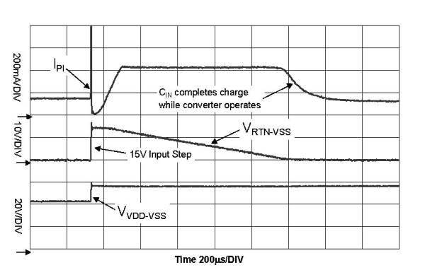
The internal hotswap MOSFET is protected against output faults with a current limit and deglitched foldback. The PSE output cannot be relied on to protect the PD MOSFET against transient conditions, requiring the PD to provide fault protection. High stress conditions include converter output shorts, shorts from VDD1 to RTN, or transients on the input line. An overload on the pass MOSFET engages the current limit, with VRTN-VSS rising as a result. If VRTN rises above approximately 12 V for longer than approximately 400 μs, the current limit reverts to the inrush limit, and turns the converter off. The 400-μs deglitch feature prevents momentary transients from causing a PD reset, provided that recovery lies within the bounds of the hotswap and PSE protection. Figure 8-5 shows an example of recovery from a 15-V PSE rising voltage step. The hotswap MOSFET goes into current limit, overshooting to a relatively low current, recovers to 420-mA, full-current limit, and charges the input capacitor while the converter continues to run. The MOSFET did not go into foldback because VRTN-VSS was below 12 V after the 400-μs deglitch.
 Figure 8-5 Response to PSE Step Voltage
The PD control has a thermal sensor that protects the internal hotswap MOSFET. Conditions like start-up or operation into a VDD to RTN short cause high power dissipation in the MOSFET. An overtemperature shutdown (OTSD) turns off the hotswap MOSFET and class regulator, which are restarted after the device cools. The PD restarts in inrush current limit when exiting from a PD overtemperature event.
Pulling DEN to VSS during powered operation causes the internal hotswap MOSFET to turn off. This feature allows a PD with secondary-side adapter ORing to achieve adapter priority. Take care with synchronous converter topologies that can deliver power in both directions.
The hotswap switch is forced off under the following conditions:
- VAPD above VAPDEN (approximately 1.5 V)
- VDEN ≤ VPD_DIS when VVDD-VSS is in the operational range
- PD over temperature
- VVDD-VSS < PoE UVLO (approximately 30.5 V)