SLVS885I October 2008 – December 2017 TPS23754 , TPS23754-1 , TPS23756
PRODUCTION DATA.
- 1 Features
- 2 Applications
- 3 Description
- 4 Revision History
- 5 Pin Configuration and Functions
- 6 Specifications
-
7 Detailed Description
- 7.1 Overview
- 7.2 Functional Block Diagram
- 7.3 Feature Description
- 7.4
Device Functional Modes
- 7.4.1
PoE Overview
- 7.4.1.1 Threshold Voltages
- 7.4.1.2 PoE Start-Up Sequence
- 7.4.1.3 Detection
- 7.4.1.4 Hardware Classification
- 7.4.1.5 Inrush and Start-Up
- 7.4.1.6 Maintain Power Signature
- 7.4.1.7 Start-Up and Converter Operation
- 7.4.1.8 PD Hotswap Operation
- 7.4.1.9 Converter Controller Features
- 7.4.1.10 Bootstrap Topology
- 7.4.1.11 Current Slope Compensation and Current Limit
- 7.4.1.12 Blanking – RBLNK
- 7.4.1.13 Dead Time
- 7.4.1.14 FRS and Synchronization
- 7.4.1.15 T2P, Start-Up, and Power Management
- 7.4.1.16 Thermal Shutdown
- 7.4.1.17 Adapter ORing
- 7.4.1.18 PPD ORing Features
- 7.4.1.19 Using DEN to Disable PoE
- 7.4.1.20 ORing Challenges
- 7.4.1
PoE Overview
-
8 Application and Implementation
- 8.1 Application Information
- 8.2
Typical Application
- 8.2.1 Design Requirements
- 8.2.2
Detailed Design Procedure
- 8.2.2.1 Input Bridges and Schottky Diodes
- 8.2.2.2 Protection, D1
- 8.2.2.3 Capacitor, C1
- 8.2.2.4 Detection Resistor, RDEN
- 8.2.2.5 Classification Resistor, RCLS
- 8.2.2.6 Dead Time Resistor, RDT
- 8.2.2.7 Switching Transformer Considerations and RVC
- 8.2.2.8 Special Switching MOSFET Considerations
- 8.2.2.9 Thermal Considerations and OTSD
- 8.2.2.10 APD Pin Divider Network, RAPD1, RAPD2
- 8.2.2.11 PPD Pin Divider Network, RPPD1, RPPD2
- 8.2.2.12 Setting Frequency (RFRS) and Synchronization
- 8.2.2.13 Current Slope Compensation
- 8.2.2.14 Blanking Period, RBLNK
- 8.2.2.15 Estimating Bias Supply Requirements and CVC
- 8.2.2.16 T2P Pin Interface
- 8.2.2.17 Advanced ORing Techniques
- 8.2.2.18 Soft Start
- 8.2.2.19 Frequency Dithering for Conducted Emissions Control
- 8.2.3 Application Curves
- 9 Power Supply Recommendations
- 10Layout
- 11Device and Documentation Support
- 12Mechanical, Packaging, and Orderable Information
Package Options
Refer to the PDF data sheet for device specific package drawings
Mechanical Data (Package|Pins)
- PWP|20
Thermal pad, mechanical data (Package|Pins)
- PWP|20
Orderable Information
7.4.1.7 Start-Up and Converter Operation
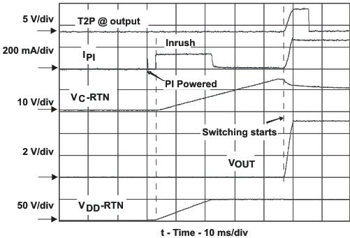
The internal PoE undervoltage lockout (UVLO) circuit holds the hotswap switch off before the PSE provides full voltage to the PD. This prevents the converter circuits from loading the PoE input during detection and classification. The converter circuits discharge CIN, CVC, and CVB while the PD is unpowered. Thus VVDD-VRTN will be a small voltage just after full voltage is applied to the PD, as seen in Figure 22. The PSE drives the PI voltage to the operating range once it has decided to power up the PD. When VVDD rises above the UVLO turnon threshold (VUVLO-R, about 35 V) with RTN high, the TPS23754 device enables the hotswap MOSFET with an approximately 140-mA (inrush) current limit as seen in Figure 24. Converter switching is disabled while CIN charges and VRTN falls from VVDD to nearly VVSS, however the converter start-up circuit is allowed to charge CVC (the bootstrap start-up capacitor). Additional loading applied between VVDD and VRTN during the inrush state may prevent successful PD and subsequent converter start-up. Converter switching is allowed if the PD is not in inrush, OTSD is not active, and the VC UVLO permits it. Once the inrush current falls about 10% less than the inrush current limit, the PD current limit switches to the operational level (about 970 mA). Continuing the start-up sequence shown in Figure 24, VVC continues to rise until the start-up threshold (VCUV, about 15 V or about 9 V) is exceeded, turning the start-up source off and enabling switching. The VB regulator is always active, powering the internal converter circuits as VVC rises. There is a slight delay between the removal of charge current and the start of switching as the soft-start ramp sweeps above the VZDC threshold. VVC falls as it powers both the internal circuits and the switching MOSFET gates. If the converter control bias output rises to support VVC before it falls to VCUV – VCUVH (about 8.5 V or about 5.5 V), a successful start-up occurs. T2P in Figure 22 (Figure 27, VT2P-OUT) becomes active within tT2P from the start of switching, indicating that a type 2 PSE or an adapter is plugged in.
 Figure 24. Power Up and Start
If VVDD- VVSS drops below the lower PoE UVLO (VUVLO-R - VUVLO-H, about 30.5 V), the hotswap MOSFET is turned off, but the converter will still run. The converter will stop if VVC falls below the converter UVLO (VCUV – VCUVH, about 8.5 V or about 5.5 V), the hotswap is in inrush current limit, 0% duty cycle is demanded by VCTL (VCTL < VZDC, about 1.5 V), or the converter is in thermal shutdown.