SLVSDW2B December 2018 – November 2020 TPS23755
PRODUCTION DATA
- 1 Features
- 2 Applications
- 3 Description
- 4 Revision History
- 5 Pin Configuration and Functions
- 6 Specifications
-
7 Detailed Description
- 7.1 Overview
- 7.2 Functional Block Diagram
- 7.3
Feature Description
- 7.3.1 CLS Classification
- 7.3.2 DEN Detection and Enable
- 7.3.3 Internal Pass MOSFET
- 7.3.4
DC-DC Controller Features
- 7.3.4.1 VCC, VB and Advanced PWM Startup
- 7.3.4.2 CS, Current Slope Compensation and Blanking
- 7.3.4.3 COMP, FB, CP and Opto-less Feedback
- 7.3.4.4 FRS Frequency Setting and Synchronization
- 7.3.4.5 Frequency Dithering for Spread Spectrum Applications
- 7.3.4.6 SST and Soft-Start of the Switcher
- 7.3.4.7 AUX_V, AUX_D and Secondary Adapter Or'ing
- 7.3.5 Internal Switching FET - DRAIN, RSNS, SRF and SRR
- 7.3.6 VPD Supply Voltage
- 7.3.7 VDD Supply Voltage
- 7.3.8 GND
- 7.3.9 VSS
- 7.3.10 Exposed Thermal PAD
- 7.4 Device Functional Modes
-
8 Application and Implementation
- 8.1 Application Information
- 8.2
Typical Application
- 8.2.1 Design Requirements
- 8.2.2
Detailed Design Procedure
- 8.2.2.1 Input Bridges and Schottky Diodes
- 8.2.2.2 Protection, D1
- 8.2.2.3 Capacitor, C1
- 8.2.2.4 Detection Resistor, RDEN
- 8.2.2.5 Classification Resistor, RCLS
- 8.2.2.6 Bulk Capacitance, CBULK
- 8.2.2.7 Output Voltage Feedback Divider, RAUX, R1,R2
- 8.2.2.8 Setting Frequency, RFRS
- 8.2.2.9 Frequency Dithering, RDTR and CDTR
- 8.2.2.10 Bias Voltage, CVB and DVB
- 8.2.2.11 Transformer design, T1
- 8.2.2.12 Current Sense Resistor, RCS
- 8.2.2.13 Current Slope Compensation, RS
- 8.2.2.14 Bias Supply Requirements, CCC, DCC
- 8.2.2.15 Switching Transformer Considerations, RVCC and CCC2
- 8.2.2.16 Primary FET Clamping, RCL, CCL, and DCL
- 8.2.2.17 Converter Output Capacitance, COUT
- 8.2.2.18 Secondary Output Diode Rectifier, DOUT
- 8.2.2.19 Slew rate control, RSRF and RSRR
- 8.2.2.20 Shutdown at Low Temperatures, DVDD and CVDD
- 8.2.3 Application Curves
- 9 Power Supply Recommendations
- 10Layout
- 11Device and Documentation Support
- 12Mechanical, Packaging, and Orderable Information
Package Options
Mechanical Data (Package|Pins)
- RJJ|23
Thermal pad, mechanical data (Package|Pins)
Orderable Information
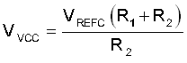
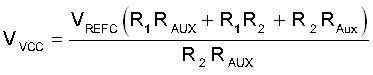
8.2.2.7 Output Voltage Feedback Divider, RAUX, R1,R2
R1, R2 and RAUX set the output voltage of the bias winding of the converter. For applications that do not use AUX_D functionality, RAUX should not be populated and Equation 5 should be used.
For secondary side adapter priority applications, the DC/DC output voltage can be set lower than the adapter voltage by pulling AUX_D to RTN. Equation 6 should be used first to determine the lower output voltage when adapter is present.
when Aux_D is LOW.
Then Raux can be calculated using Equation 7 to set the nominal output voltage of the bias winding.
when Aux_D is HIGH.
When transitioning from the normal operating output voltage to a lower output voltage when Aux_D is pulled LOW, switching may stop until the VCC voltage can reduce its voltage to the lower VCC voltage. The output voltage may drop during this time due to the loss of switching. Typically this is not a concern since the adapter is providing power to the load. A combination of adding a dummy load in parallel with CCC and increasing the secondary output capacitance can minimize the time that switching stops.
In applications that use smooth transition between adapter the PoE, circuitry should be added to keep the PSE connected to the PD and the converter operational while maintaining adapter priority. It is recommended to refer to the TPS23755EVM-894.