SLUSBX9I March 2014 – July 2019 TPS23861
PRODUCTION DATA.
- 1 Features
- 2 Applications
- 3 Description
- 4 Revision History
- 5 Pin Configuration and Functions
- 6 Specifications
-
7 Detailed Description
- 7.1 Overview
- 7.2 Functional Block Diagram
- 7.3
Feature Description
- 7.3.1 Detection Resistance Measurement
- 7.3.2 Physical Layer Classification
- 7.3.3 Class and Detect Fields
- 7.3.4 Register State Following a Fault
- 7.3.5 Disconnect
- 7.3.6 Disconnect Threshold
- 7.3.7 Fast Shutdown Mode
- 7.3.8 Legacy Device Detection
- 7.3.9 VPWR Undervoltage and UVLO Events
- 7.3.10 Timer-Deferrable Interrupt Support
- 7.3.11 A/D Converter and I2C Interface
- 7.3.12 Independent Operation when the AUTO Bit is Set
- 7.3.13 I2C Slave Address and AUTO Bit Programming
- 7.4 Device Functional Modes
- 7.5
Register Map – I2C-Addressable
- 7.5.1 Interrupt Register
- 7.5.2 Interrupt Enable Register
- 7.5.3 Power Event Register
- 7.5.4 Detection Event Register
- 7.5.5 Fault Event Register
- 7.5.6 Start/ILIM Event Register
- 7.5.7 Supply Event Register
- 7.5.8 Port n Status Register
- 7.5.9 Power Status Register
- 7.5.10 I2C Slave Address Register
- 7.5.11 Operating Mode Register
- 7.5.12 Disconnect Enable Register
- 7.5.13 Detect/Class Enable Register
- 7.5.14 Port Power Priority Register
- 7.5.15 Timing Configuration Register
- 7.5.16 General Mask 1 Register
- 7.5.17 Detect/Class Restart Register
- 7.5.18 Power Enable Register
- 7.5.19 Reset Register
- 7.5.20 Legacy Detect Mode Register
- 7.5.21 Two-Event Classification Register
- 7.5.22 Interrupt Timer Register
- 7.5.23 Disconnect Threshold Register
- 7.5.24 ICUTnm CONFIG Register
- 7.5.25 Temperature Register
- 7.5.26 Input Voltage Register
- 7.5.27 Port n Current Register
- 7.5.28 Port n Voltage Register
- 7.5.29 PoE Plus Register
- 7.5.30 Firmware Revision Register
- 7.5.31 I2C Watchdog Register
- 7.5.32 Device ID Register
- 7.5.33 Cool Down/Gate Drive Register
- 7.5.34 Port n Detect Resistance Register
- 7.5.35 Port n Detect Voltage Difference Register
- 7.5.36 Reserved Registers
-
8 Application and Implementation
- 8.1 Introduction to PoE
- 8.2 Application Information
- 8.3 Typical Application
- 8.4 System Examples
- 9 Power Supply Recommendations
- 10Layout
- 11Device and Documentation Support
- 12Mechanical, Packaging, and Orderable Information
Package Options
Mechanical Data (Package|Pins)
- PW|28
Thermal pad, mechanical data (Package|Pins)
- PW|28
Orderable Information
8.2 Application Information
The TPS23861 is a four port, IEEE 802.3at PoE PSE controller and can be used in very simple, low port count, automatic or high port count micro-controller managed applications.
Subsequent sections describe detailed design procedures for applications with different requirements including host control.
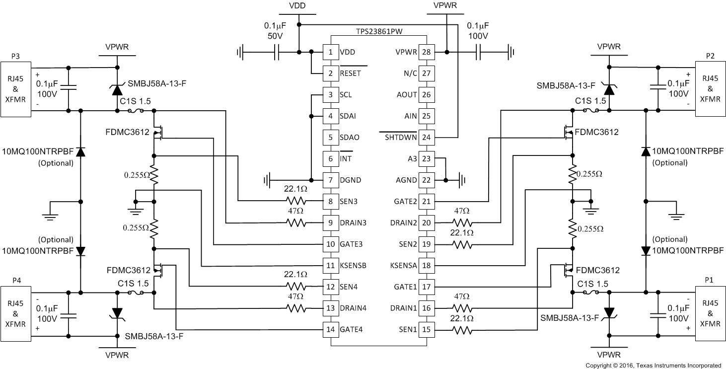
The schematic of Figure 46 depicts automatic mode operation of the TPS23861, providing turnkey functionality ready to power PoE loads. No connection to the I2C bus or any type of host control is required. In Figure 46 the TPS23861 automatically:
- Performs load detection.
- Performs classification including type-2 (two-finger) of up to Class 4 loads.
- Enables power with protective foldback current limiting, and ICUT value based on load class.
- Shuts down in the event of fault loads and shorts.
- Performs Maintain Power Signature function to ensure removal of power if load is disconnected.
- Undervoltage lock out occurs if VPWR falls below VPUV_F (typical 26.5 V).
Following a power-off command, disconnect or shutdown due to a start, ICUT or ILIM fault, the port powers down. Following port power off due to a power off command or disconnect, the TPS23861 continues automatic operation starting with a detection cycle. If the shutdown is due to a start, ICUT or ILIM fault, the TPS23861 enters into a cool-down period. After the end of the cool-down period the TPS23861 continues automatic operation starting with a detection cycle.
The TPS23861 will not automatically apply power to a port under the following circumstances:
- The detect status is not Resistance Valid.
- If the classification status is overcurrent, class mismatch, or unknown.
