SLUSBX9I March 2014 – July 2019 TPS23861
PRODUCTION DATA.
- 1 Features
- 2 Applications
- 3 Description
- 4 Revision History
- 5 Pin Configuration and Functions
- 6 Specifications
-
7 Detailed Description
- 7.1 Overview
- 7.2 Functional Block Diagram
- 7.3
Feature Description
- 7.3.1 Detection Resistance Measurement
- 7.3.2 Physical Layer Classification
- 7.3.3 Class and Detect Fields
- 7.3.4 Register State Following a Fault
- 7.3.5 Disconnect
- 7.3.6 Disconnect Threshold
- 7.3.7 Fast Shutdown Mode
- 7.3.8 Legacy Device Detection
- 7.3.9 VPWR Undervoltage and UVLO Events
- 7.3.10 Timer-Deferrable Interrupt Support
- 7.3.11 A/D Converter and I2C Interface
- 7.3.12 Independent Operation when the AUTO Bit is Set
- 7.3.13 I2C Slave Address and AUTO Bit Programming
- 7.4 Device Functional Modes
- 7.5
Register Map – I2C-Addressable
- 7.5.1 Interrupt Register
- 7.5.2 Interrupt Enable Register
- 7.5.3 Power Event Register
- 7.5.4 Detection Event Register
- 7.5.5 Fault Event Register
- 7.5.6 Start/ILIM Event Register
- 7.5.7 Supply Event Register
- 7.5.8 Port n Status Register
- 7.5.9 Power Status Register
- 7.5.10 I2C Slave Address Register
- 7.5.11 Operating Mode Register
- 7.5.12 Disconnect Enable Register
- 7.5.13 Detect/Class Enable Register
- 7.5.14 Port Power Priority Register
- 7.5.15 Timing Configuration Register
- 7.5.16 General Mask 1 Register
- 7.5.17 Detect/Class Restart Register
- 7.5.18 Power Enable Register
- 7.5.19 Reset Register
- 7.5.20 Legacy Detect Mode Register
- 7.5.21 Two-Event Classification Register
- 7.5.22 Interrupt Timer Register
- 7.5.23 Disconnect Threshold Register
- 7.5.24 ICUTnm CONFIG Register
- 7.5.25 Temperature Register
- 7.5.26 Input Voltage Register
- 7.5.27 Port n Current Register
- 7.5.28 Port n Voltage Register
- 7.5.29 PoE Plus Register
- 7.5.30 Firmware Revision Register
- 7.5.31 I2C Watchdog Register
- 7.5.32 Device ID Register
- 7.5.33 Cool Down/Gate Drive Register
- 7.5.34 Port n Detect Resistance Register
- 7.5.35 Port n Detect Voltage Difference Register
- 7.5.36 Reserved Registers
-
8 Application and Implementation
- 8.1 Introduction to PoE
- 8.2 Application Information
- 8.3 Typical Application
- 8.4 System Examples
- 9 Power Supply Recommendations
- 10Layout
- 11Device and Documentation Support
- 12Mechanical, Packaging, and Orderable Information
Package Options
Mechanical Data (Package|Pins)
- PW|28
Thermal pad, mechanical data (Package|Pins)
- PW|28
Orderable Information
7.4.4 Auto
In Auto Mode the TPS23861 automatically cycles the port through detection, classification and power on. The ICUT and PoEP fields are set automatically based on the classification status. If a class 0, 1, 2 or 3 PD is recognized, ICUTn is set to 000 (374 mA) and the PoEPn bit is cleared. If a class 4 PD is recognized, ICUTn is set to 110 (645 mA) and the PoEPn bit is set. Auto Mode and the AUTO bit are related, but are not identical. When the Bit is set, all ports are placed in Auto Mode; additionally, several other registers are set. See Independent Operation when the AUTO Bit is Set section.
Following a power-off command, disconnect or shutdown due to a Start, ICUT or ILIM fault, the port powers off. Following port power off due to a power off command or disconnect, the TPS23861 continues automatic operation starting with a detection cycle (if DETEn is set). If the shutdown is due to a Start, ICUT or ILIM fault, the TPS23861 enters into a cool-down period. During the cool-down period any port power-on command using Power Enable Command is ignored. The length of the cool-down period is set in the CLDN field of the Cool Down/Gate Drive Register. After the end of the cool-down period the TPS23861 continues automatic operation starting with a detection cycle, assuming DETEn is set.
The TPS23861 will not automatically apply power to a port, even if Operating Mode is set to Auto, under the following circumstances.
- The detect status is not Resistance Valid. This means that the DETEn bit must be set in order to power on in Auto Mode.
- If the classification status is overcurrent or, class mismatch.
NOTE
A write to the DETEn bit or CLEn bit will not stick if the port is in Off Mode.
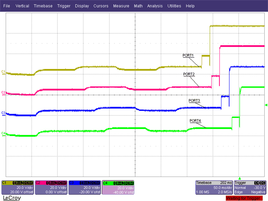
The TPS23861 starts in Auto Mode after a power-on reset or when the RESET pin is de-asserted. When a valid PD is connected as TPS23861 comes out of reset, then the ports will sequence through detection, classification, and power on as shown in Figure 44. Staggered port power on prevents the sudden inrush of current from the VPWR supply when multiple PDs are already connected.
 Figure 44. Port Sequencing after RESET Pin De-Assertion