SLUSBX9I March   2014  – July 2019 TPS23861

PRODUCTION DATA.  

  1. Features
  2. Applications
  3. Description
    1.     Device Images
      1.      Simplified Schematic
  4. Revision History
  5. Pin Configuration and Functions
    1.     Pin Functions
  6. Specifications
    1. 6.1 Absolute Maximum Ratings
    2. 6.2 ESD Ratings
    3. 6.3 Recommended Operating Conditions
    4. 6.4 Thermal Information
    5. 6.5 Electrical Characteristics
    6. 6.6 Timing Requirements
    7. 6.7 Switching Characteristics
    8. 6.8 Typical Characteristics
  7. Detailed Description
    1. 7.1 Overview
      1. 7.1.1 Detailed Pin Description
      2. 7.1.2 I2C Detailed Pin Description
    2. 7.2 Functional Block Diagram
    3. 7.3 Feature Description
      1. 7.3.1  Detection Resistance Measurement
      2. 7.3.2  Physical Layer Classification
      3. 7.3.3  Class and Detect Fields
      4. 7.3.4  Register State Following a Fault
      5. 7.3.5  Disconnect
      6. 7.3.6  Disconnect Threshold
      7. 7.3.7  Fast Shutdown Mode
      8. 7.3.8  Legacy Device Detection
      9. 7.3.9  VPWR Undervoltage and UVLO Events
      10. 7.3.10 Timer-Deferrable Interrupt Support
      11. 7.3.11 A/D Converter and I2C Interface
      12. 7.3.12 Independent Operation when the AUTO Bit is Set
      13. 7.3.13 I2C Slave Address and AUTO Bit Programming
    4. 7.4 Device Functional Modes
      1. 7.4.1 Off
      2. 7.4.2 Manual
      3. 7.4.3 Semi-Auto
      4. 7.4.4 Auto
      5. 7.4.5 Push-Button Power On Response
      6. 7.4.6 TSTART Indicators of Detect and Class Failures
      7. 7.4.7 Device Power On Initialization
    5. 7.5 Register Map – I2C-Addressable
      1. 7.5.1  Interrupt Register
      2. 7.5.2  Interrupt Enable Register
      3. 7.5.3  Power Event Register
      4. 7.5.4  Detection Event Register
      5. 7.5.5  Fault Event Register
      6. 7.5.6  Start/ILIM Event Register
      7. 7.5.7  Supply Event Register
      8. 7.5.8  Port n Status Register
        1. 7.5.8.1 Port 1 Status Register
        2. 7.5.8.2 Port 2 Status Register
        3. 7.5.8.3 Port 3 Status Register
        4. 7.5.8.4 Port 4 Status Register
      9. 7.5.9  Power Status Register
      10. 7.5.10 I2C Slave Address Register
      11. 7.5.11 Operating Mode Register
      12. 7.5.12 Disconnect Enable Register
      13. 7.5.13 Detect/Class Enable Register
      14. 7.5.14 Port Power Priority Register
      15. 7.5.15 Timing Configuration Register
      16. 7.5.16 General Mask 1 Register
      17. 7.5.17 Detect/Class Restart Register
      18. 7.5.18 Power Enable Register
      19. 7.5.19 Reset Register
      20. 7.5.20 Legacy Detect Mode Register
      21. 7.5.21 Two-Event Classification Register
      22. 7.5.22 Interrupt Timer Register
      23. 7.5.23 Disconnect Threshold Register
        1. 7.5.23.1 Bits Description
      24. 7.5.24 ICUTnm CONFIG Register
        1. 7.5.24.1 ICUT21 CONFIG Register
        2. 7.5.24.2 ICUT43 CONFIG Register
        3. 7.5.24.3 Bits Description
      25. 7.5.25 Temperature Register
      26. 7.5.26 Input Voltage Register
      27. 7.5.27 Port n Current Register
        1. 7.5.27.1 Port 1 Current Register
        2. 7.5.27.2 Port 2 Current Register
        3. 7.5.27.3 Port 3 Current Register
        4. 7.5.27.4 Port 4 Current Register
      28. 7.5.28 Port n Voltage Register
        1. 7.5.28.1 Port 1 Voltage Register
        2. 7.5.28.2 Port 2 Voltage Register
        3. 7.5.28.3 Port 3 Voltage Register
        4. 7.5.28.4 Port 4 Voltage Register
      29. 7.5.29 PoE Plus Register
      30. 7.5.30 Firmware Revision Register
      31. 7.5.31 I2C Watchdog Register
      32. 7.5.32 Device ID Register
      33. 7.5.33 Cool Down/Gate Drive Register
      34. 7.5.34 Port n Detect Resistance Register
        1. 7.5.34.1 Port 1 Detect Resistance Register
          1. 7.5.34.1.1 Port 2 Detect Resistance Register
          2. 7.5.34.1.2 Port 3 Detect Resistance Register
          3. 7.5.34.1.3 Port 4 Detect Resistance Register
      35. 7.5.35 Port n Detect Voltage Difference Register
        1. 7.5.35.1 Port 1 Detect Voltage Difference Register
        2. 7.5.35.2 Port 2 Detect Voltage Difference Register
        3. 7.5.35.3 Port 3 Detect Voltage Difference Register
        4. 7.5.35.4 Port 4 Detect Voltage Difference Register
      36. 7.5.36 Reserved Registers
  8. Application and Implementation
    1. 8.1 Introduction to PoE
    2. 8.2 Application Information
      1. 8.2.1 Kelvin Current Sensing Resistor
      2. 8.2.2 Connections on Unused Ports
    3. 8.3 Typical Application
      1. 8.3.1 Two Port, Auto Mode Application with External Port Reset
        1. 8.3.1.1 Design Requirements
      2. 8.3.2 Four Port, Auto Mode Application
        1. 8.3.2.1 Design Requirements
      3. 8.3.3 Eight Port, Semi-Auto Mode Application Using MSP430 Micro-Controller
        1. 8.3.3.1 Design Requirements
      4. 8.3.4 Detailed Design Procedure
        1. 8.3.4.1 Power Pin Bypass Capacitors
        2. 8.3.4.2 Per Port Components
        3. 8.3.4.3 System Level Components (not shown in the schematic diagrams)
      5. 8.3.5 Application Curves
    4. 8.4 System Examples
      1. 8.4.1 Overcurrent and Overload Protection
      2. 8.4.2 Inrush Protection
      3. 8.4.3 ICUT Current Limit
      4. 8.4.4 Foldback Protection (ILIM)
      5. 8.4.5 Kelvin Current Sensing Resistor
  9. Power Supply Recommendations
    1. 9.1 VDD
    2. 9.2 VPWR
    3. 9.3 VPWR-RESET Sequencing
  10. 10Layout
    1. 10.1 Layout Guidelines
      1. 10.1.1 Port Current Kelvin Sensing
    2. 10.2 Layout Example
      1. 10.2.1 Component Placement and Routing Guidelines
        1. 10.2.1.1 Power Pin Bypass Capacitors
        2. 10.2.1.2 Per-Port Components
  11. 11Device and Documentation Support
    1. 11.1 Documentation Support
      1. 11.1.1 Related Documentation
    2. 11.2 Receiving Notification of Documentation Updates
    3. 11.3 Community Resources
    4. 11.4 Trademarks
    5. 11.5 Electrostatic Discharge Caution
    6. 11.6 Glossary
  12. 12Mechanical, Packaging, and Orderable Information

Package Options

Mechanical Data (Package|Pins)
Thermal pad, mechanical data (Package|Pins)
Orderable Information

Typical Characteristics
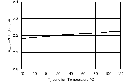
TPS23861 C001_lusbw2.png
Figure 7. VDD UVLO vs Junction Temperature
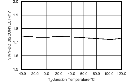
TPS23861 C003_lusbw2.png
Figure 9. DC Disconnect vs Junction Temperature
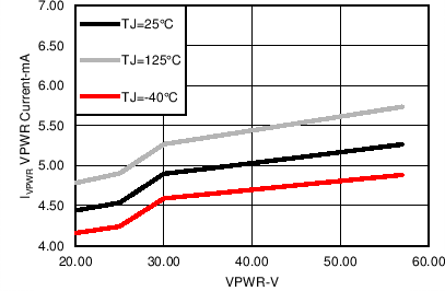
TPS23861 C005_lusbw2.png
Figure 11. VPWR Current vs VPWR
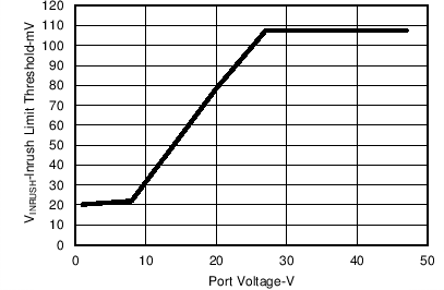
TPS23861 C007_lusbw2.png
Figure 13. Inrush Current Limit Threshold vs Port Voltage
TPS23861 C009new_lusbw2.png
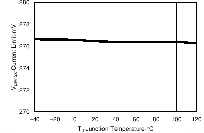
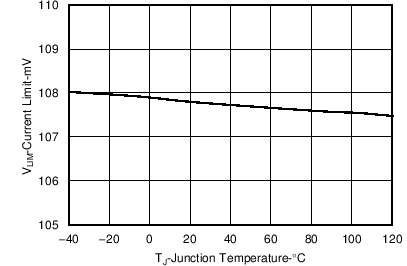
Figure 15. Current Limit (2x threshold) vs Junction Temperature
TPS23861 fig16_lusba4.gif
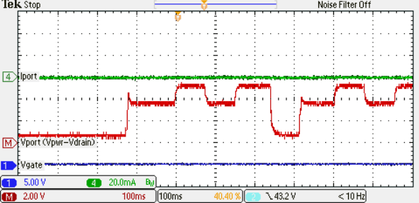
Figure 17. Valid PD Detection (25 kΩ and 0.1 µF) and CLASS 0 Classification
TPS23861 fig18_lusba4.gif
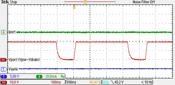
Figure 19. Detection with Invalid PD (15 kΩ and 0.1 µF)
TPS23861 fig20_lusba4.gif
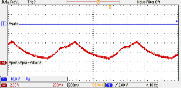
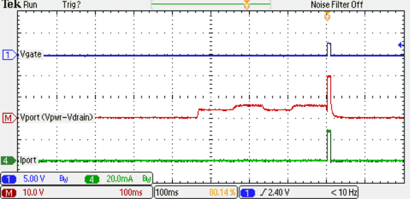
Figure 21. Detection with Invalid PD (25 kΩ and 10 µF)
TPS23861 fig22_lusba4.gif
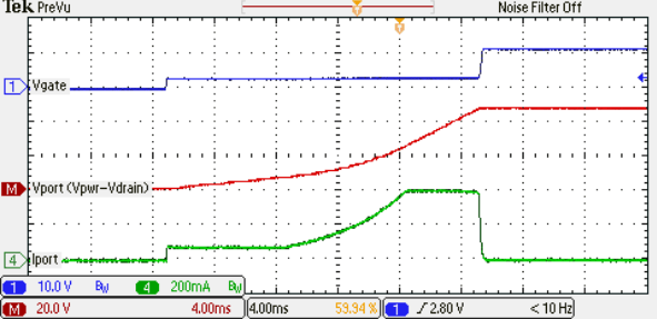
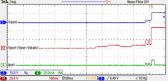
Figure 23. Powering Up Into a 100-µF Load
TPS23861 fig21_lusbw2.gif
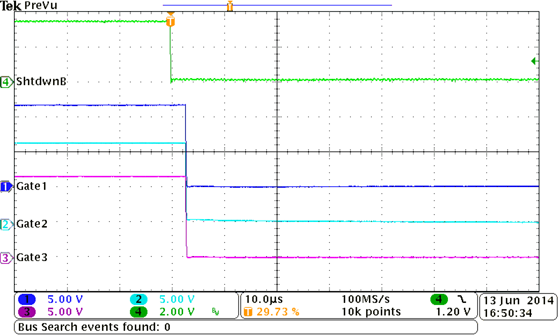
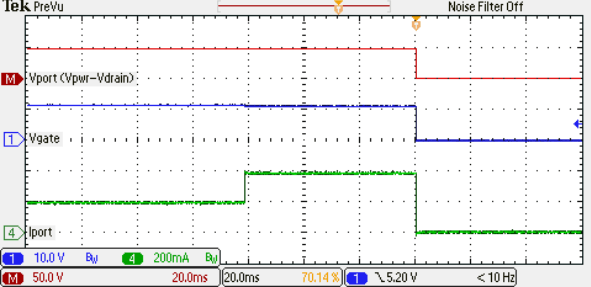
Figure 25. All Ports Fast Shutdown
TPS23861 fig26_lusba4.gif
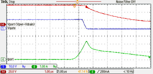
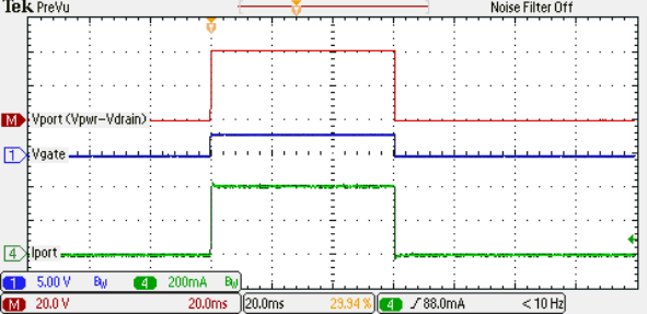
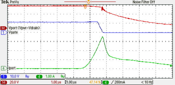
Figure 27. Rapid Response to a 1-Ω Short: 802.3af Mode
TPS23861 fig28_lusba4.gif
Figure 29. Response to a 50-Ω Load: 802.3af Mode
TPS23861 fig30_lusba4.gif
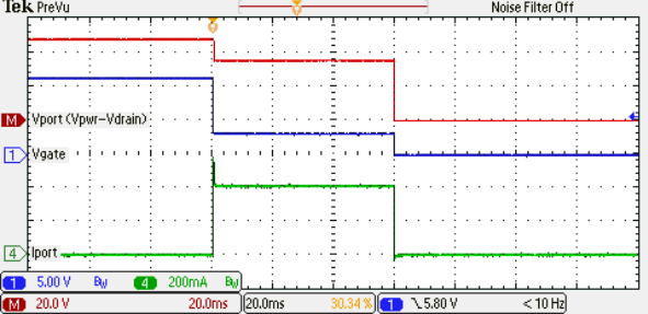
Figure 31. Current Limit Timeout: 802.3af Mode, 85-Ω Load
TPS23861 fig32_lusba4.gif
Figure 33. Inrush Fault Timeout: 100-Ω Load
TPS23861 fig34_lusba4.gif
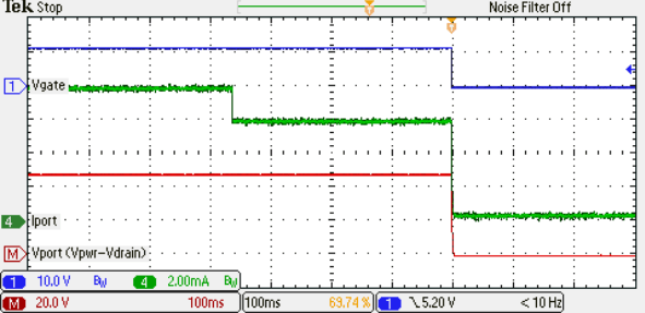
Figure 35. Response to 8-mA to 6-mA Load, DC Disconnect Enabled
TPS23861 C002_lusbw2.png
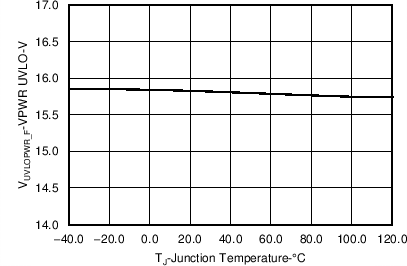
Figure 8. VPWR UVLO vs Junction Temperature
TPS23861 C004_lusbw2.png
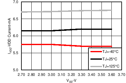
Figure 10. VDD Current vs VDD
TPS23861 C006_lusbw2.png
Figure 12. Current Limit (1x threshold) vs Junction Temperature
TPS23861 C008_lusbw2.png
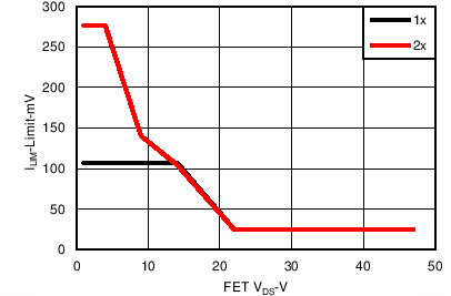
Figure 14. Current Limit Threshold vs FET Voltage
TPS23861 C010_lusbw2.png
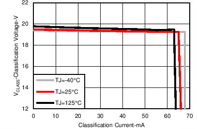
Figure 16. Classification Voltage vs Port Classification Current
TPS23861 fig17_lusba4.gif
Figure 18. Valid PD Detection (25 kΩ and 0.1 µF) and CLASS 3 Classification
TPS23861 fig19_lusba4.gif
Figure 20. Detection with Invalid PD (open circuit)
TPS23861 fig21_lusba4.gif
Figure 22. 2-Event Class and Startup with Valid PD
TPS23861 fig19_lusbw2.gif
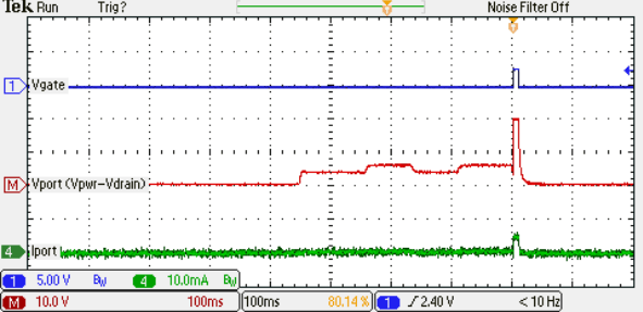
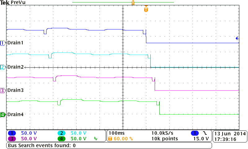
Figure 24. Semi-Auto Sequenced Turn On
TPS23861 fig25_lusba4.gif
Figure 26. Overcurrent (ICUT) Timeout
TPS23861 fig27_lusba4.gif
Figure 28. Rapid Response to a 1-Ω Short: PoE+ Mode
TPS23861 fig29_lusba4.gif
Figure 30. Response to a 25-Ω Load: PoE+ Mode
TPS23861 fig31_lusba4.gif
Figure 32. Current Limit 15-ms Timeout: PoE+ Mode, 45-Ω Load
TPS23861 fig33_lusba4.gif
Figure 34. Current Limit Timeout Restart Delay